
 English
Enhanced with AI, wearables are ready to fulfil their promise to transform daily life and work. The time is right for widespread adoption, confirmed in new concepts breaking cover at January’s CES 2026 in Las Vegas. The latest designs combine features that users understand and value, packaged in form factors that are slim, stylish, comfortable, and practicable, essential qualities for widespread market appeal.
As a case in point, the resurgence of consumer smart glasses builds on the experience gained from early models piloted in the 2010s. Despite muted response from consumers, industrial applications flourished by giving workers context-specific information about equipment and processes - helping to enhance quality, prevent errors, and boost productivity.
Opportunities for consumer smart glasses are now reopening as edge AI integration enables powerful new features that provide needed support for routine activities. Highlights include reading assistance, such as instantaneous language translation, and help while on the move like GPS guidance enhanced with local visitor information and finding nearby amenities. Just as important is the sleek, lightweight styling – a notable aspect of the new generation of smart glasses demonstrated at CES this year - that creates desirability. This is enabled by today’s miniaturized, ultra-low-power electronics including high-density, low-power memory. Recent advancements in both Flash and DRAM have proven especially effective.
Memory for Smart Glasses
When designing smart glasses, engineers must integrate displays, sensors, and connectivity within strict power, thermal, and space constraints. The frame must remain slim and lightweight, limiting both PCB area and component height. While users expect long battery life, the frame imposes size constraints that allow for only a small number of cells. On the other hand, lag-free system response is needed to prevent delays in display rendering or sensor feedback from degrading the user experience.
With these factors in mind, the memory subsystem is one of the most critical design elements in the quest to balance capacity, power consumption, and responsiveness in extremely compact architectures. From system boot and sensor management to wireless communication and display rendering, the memory’s physical size and weight, read and write speeds, and efficiency directly influence the appearance, wearability, and performance of the glasses.
Low-Voltage Flash
Low-voltage QSPI NOR Flash operating at 1.8V provides compact, energy-efficient non-volatile storage for code and parameters. Operating at reduced voltage allows direct sharing of power rails with low-core-voltage processors, simplifying power distribution and improving overall system efficiency.
Furthermore, this NOR Flash supports industrial-grade high-temperature environments up to 105°C. Its versatility extends to emerging fields such as edge computing and AI applications, particularly in industrial and computing environments where high temperatures are common. It is designed to support high workloads driven by AI and high-performance computing (HPC).

Now, the 1.2V Both power savings and miniaturization are primary targets for designers of battery-powered wearables, as smaller devices that require less frequent charging deliver a superior user experience.

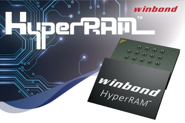
Raising DRAM Performance
Winbond’s HYPERRAMTM supports the HyperBus interface and delivers a low-power, high-throughput memory that replaces conventional DRAM or pSRAM in space-constrained systems. HYPERRAM™ provides external working memory for devices that manage sensor data, graphical displays, or wireless stacks. Since HYPERRAM™ operates with only 13 signals, it consumes less energy and uses fewer pins than conventional DRAM or pSRAM. This simplifies PCB routing, lowering design complexity, manufacturing costs, and overall board area. Standby and hybrid sleep currents typically fall in the range of tens of microwatts to support long battery life in portable systems. Density options range from 32Mb to 256Mb, allowing designers to tailor working memory capacity to processing needs. WLCSP and fine pitch BGA packages allow space saving and miniaturization.
HYPERRAM™ supports throughput up to 400MB/s and consumes less than 50mW in operation and 35µW at 1.8V in hybrid sleep mode. By bringing the performance and efficiency to buffer data from sensors and displays in real time, the fast read and write access supports frame buffering, image processing, and wireless stack management without the energy penalty associated with conventional DRAM.

Together, ultra-low voltage QSPI NOR Flash and HYPERRAM™ create a memory architecture optimized for compact, energy-constrained systems. The combination supports responsive display performance, efficient data handling, and extended battery life, enabling engineers to meet the mechanical, electrical, and power requirements that define next-generation smart glasses.
Example: W25Q32JWBYIQ in Smart Glasses
Aiming to create pace-setting new smart glasses to address this emerging market, Winbond’s W25Q32JWBYIQ QSPI NOR Flash can store system firmware, calibration data, configuration settings, and graphical assets. Operating from a nominal 1.8V, and with 32Mb storage density, this WLCSP Flash has an ultra-low profile that allows flexibility when positioning memory within the narrow arms of eyewear frames. Support for high-frequency Quad SPI mode ensures fast data throughput and execute-in-place functionality that saves time-consuming fetch and decode sequences.
Compared to the previous generation, W25Q32JWBYIQ read speeds are approximately 30% faster, while erase times are reduced by nearly half. This further accelerates the efficiency of over-the-air (OTA) exchanges, permitting "faster and shorter" firmware updates. In addition, up to 66% lower read power contributes to longer battery life and helps alleviate "power continuous anxiety," which is crucial for wearables like AI glasses.

Design Considerations for Wearable Integration
Effective power domain planning is essential when integrating memory into wearable systems. Using 1.2V QSPI NOR Flash aligns with the processor’s core voltage rails and reduces the number of regulators required. Package selection also plays a critical role. WLCSP and USON packages allow both flash and RAM to be placed in otherwise unusable spaces.
Signal integrity must be carefully maintained for both SPI and HyperBus interfaces, particularly at higher clock frequencies. Matched impedance, short trace lengths, and solid ground references help ensure reliable high-speed communication. Firmware should actively manage low power states by placing both flash and RAM into deep sleep when the system is idle. Leveraging the ultra-low standby currents of modern NOR Flash and HYPERRAM™ significantly extends battery life.
Memory density must be carefully chosen. Overprovisioning adds cost and wastes board area, while undersizing can create data bottlenecks in sensor fusion or display buffering. Workload profiling helps identify the optimal density for each application. Thermal and ergonomic factors must also be considered, since many wearables operate close to the skin.
Conclusion
Designing wearables such as smart glasses is ultimately an exercise in constraint management. Engineers must extract maximum performance from minimal power and space while ensuring a seamless user experience. A compact architecture, low energy operation, and fast response define success.
Ultra-low voltage QSPI NOR Flash provides the efficient code storage these devices depend on, while HYPERRAM™ delivers fast, low power working memory for continuous data processing. Together, these technologies help designers overcome the physical and electrical barriers to wearable innovation and bring new generations of intelligent, lightweight, and longer-lasting devices to market.
Technical Articles
-

Choosing the Right Flash Memory for AI Endpoint Applications
-

Closing the security gap left by conventional NOR Flash ICs
-

Check connection between SOC and DRAM with IC Boundary Scan Technology
-

How efficient memory solutions can help designers of IoT nodes meet tight BoM cost targets
-

New lower-cost memory solution for 5G cellular modems helps drive adoption of ultra-fast wireless broadband
-

QspiNAND with ultra-fast write speed: A new option for over-the-air updating of automotive code
-

The keys to successful adoption of new low-voltage memory ICs
-

The New Role of Storage Manufacturers in the Metaverse
-

Three mega-trends for a post-Covid world, and how they affect users of memory technology
-
What You Need to Know about HyperRAM™ – An Alternative Memory Option
-

Redefining Memory for AI: High-Bandwidth, Low-Latency Solutions for Next-Gen Computing
-

A better high-density storage option for sophisticated automotive display applications