Today, the circuitry on the board in mainstream industrial and consumer products operates from a wide range of supply voltages: the power rails are most commonly at 5V, 3V, 2.5V, 1.8V and various lower voltages. To ensure compatibility between devices from different manufacturers, and to avoid unnecessarily complicating board-level power system design, merchant semiconductor manufacturers typically design their standard products to run from one or more of these standard power rails. But there is a strong force resisting this general preference for stability and compatibility. It can be summed up in one word: mobility.
The consumer love affair with mobile and wearable devices shows no sign of fading. In mobile products, the size and weight of the battery is one of the most difficult and challenging design constraints: a smaller battery allows the designer to shrink the end product design, or to use the saved space to add valuable features. But at the same time, users pay close attention to battery run-time, and show a strong preference for products that require less frequent charging.
So every milliwatt saved from the power budget is important to product designers. And for them, the industry’s use of power rails at various standard voltages, often at 1.8V or higher, is a problem, not an advantage: that is because many components – particularly those operating in the digital domain – would with some modification be quite capable of operating from a power rail at a voltage lower than 1.8V, resulting in valuable savings in active and stand-by power consumption.
Pressure is building on semiconductor manufacturers, then, to respond to their customers’ demand to support operation at lower voltages. So how is the electronics component industry likely to accomplish any move to a lower voltage standard? And how should system designers be preparing now to take advantage of a new generation of lower-voltage component offerings?
Clear direction of travel
Today, system designers typically have to provide multiple power rails in order to accommodate components operating from different supply voltages. Analogue devices such as sensors commonly have a 3V or – in industrial applications – even a 5V supply. Legacy digital components might have a 3.3V, 2.5V or 1.8V supply. At the low end of the voltage range, the latest applications processors or systems-on-chip built on advanced process nodes, such as 28nm or smaller, might have a core operating voltage as low as 1.0V.
Yet in power system design, as in any field of design engineering, complexity is inherently undesirable, and in general, the fewer the power rails the better. This means that the industry will eventually want to settle on standard voltages at a level below 1.8V. What will these voltages be?
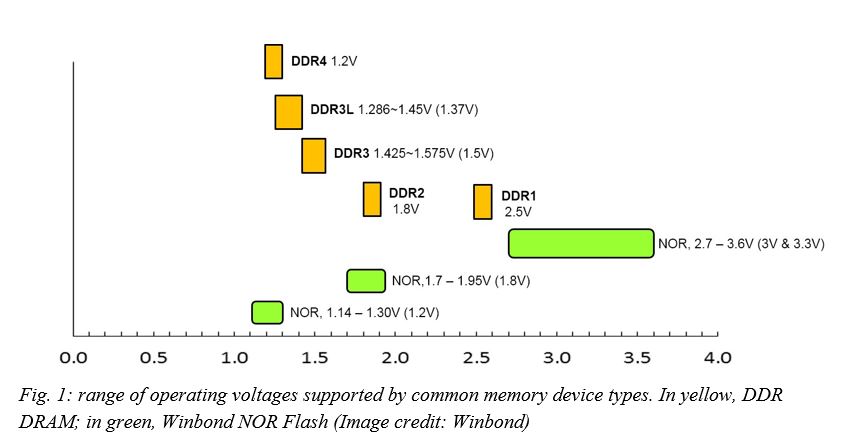
Figure 1 shows how DRAM technologies have led the memory IC industry beyond 1.8V. Standard DDR2 DRAM was the last to use a 1.8V supply. After that, successive generations of DDR DRAM operated at 1.5V (DDR3), then 1.37V (DDR3L) before reaching today’s level, 1.2V (DDR4).
Fig. 1: range of operating voltages supported by common memory device types. In yellow, DDR DRAM; in green, Winbond NOR Flash (Image credit: Winbond)
So for DRAM, there are three intermediate voltages below 1.8V. Figure 1 also shows in green the supply requirements of successive families of NOR Flash ICs from Winbond, operating at the standard 3V, 2.5V and 1.8V levels. Now the latest NOR Flash families offer two voltage ranges: one at 1.2V, and another with an extended voltage range nominally at 1.5V.
The W25QxxNE series is available to support a supply voltage from 1.14V to 1.30V. The W25QxxND series is offered at the ‘extended 1.5V’ level, operating over a range from 1.14V to 1.58V. Both product series will be provided in densities ranging from 1Mbit to 128Mbits.
In supporting the 1.2V voltage and the extended 1.5V level with its newest generation of NOR Flash ICs, Winbond is seeking to harmonise its product offerings with the broader semiconductor industry. For the industry at large, the 1.2V level makes sense: the drop from 1.8V is sufficient to offer worthwhile savings in power consumption. At the intermediate voltages of 1.5V and 1.35V covered by the extended 1.5V series, Winbond offers a strategic product that matches the power supply and I/O voltage level used by DDR3 and DDR3L DRAM products. The wider voltage range can also take advantage of the end-point voltage of popular 1.5V batteries when fully discharged.
These new offerings from Winbond are consistent with a general move by the semiconductor industry to run off power rails at voltage levels below 1.8V, with widespread support among customers for 1.2V. Several technology companies and semiconductor manufacturers have a roadmap for system power supplies that processors and memory products will support. This roadmap forecasts a reduction in the use of the 3.3V power rail, and a near-term standardisation on 1.8V. But the low-power requirements of mobility are important to technology companies and semiconductor suppliers alike, and the roadmap also sees emerging support for 1.5V, 1.35V, and 1.2V as the next voltage levels after 1.8V, and eventual industry-wide standardisation at 1.2V.
Winbond is the world’s biggest supplier of serial NOR and serial NAND Flash by value and volume, and so has some influence over the direction of industry standardisation in the serial Flash sector. With the introduction of the W25QxxNE and W25QxxND series, Winbond has demonstrated the technical feasibility of producing high-performance serial Flash ICs that operate from supply voltages as low as 1.2V. OEMs which use serial Flash should therefore feel confident in preparing their roadmaps for broad availability of 1.2V and extended 1.5V serial NOR parts.
Substantial active power savings
The amount of power which can be saved by operating serial NOR Flash ICs at a voltage lower than 1.8V depends, of course, on the application. Typical examples of end product types that might use ultra-low power serial Flash include handheld point-of-sale machines, smart watches, e-books and GPS navigation devices. In each of these, it would be normal to model the power budget for a low duty cycle of between 0.5% and 5%, consistent with typical user behaviour. This means that both stand-by power consumption and active power consumption have an important effect on total average power consumption.
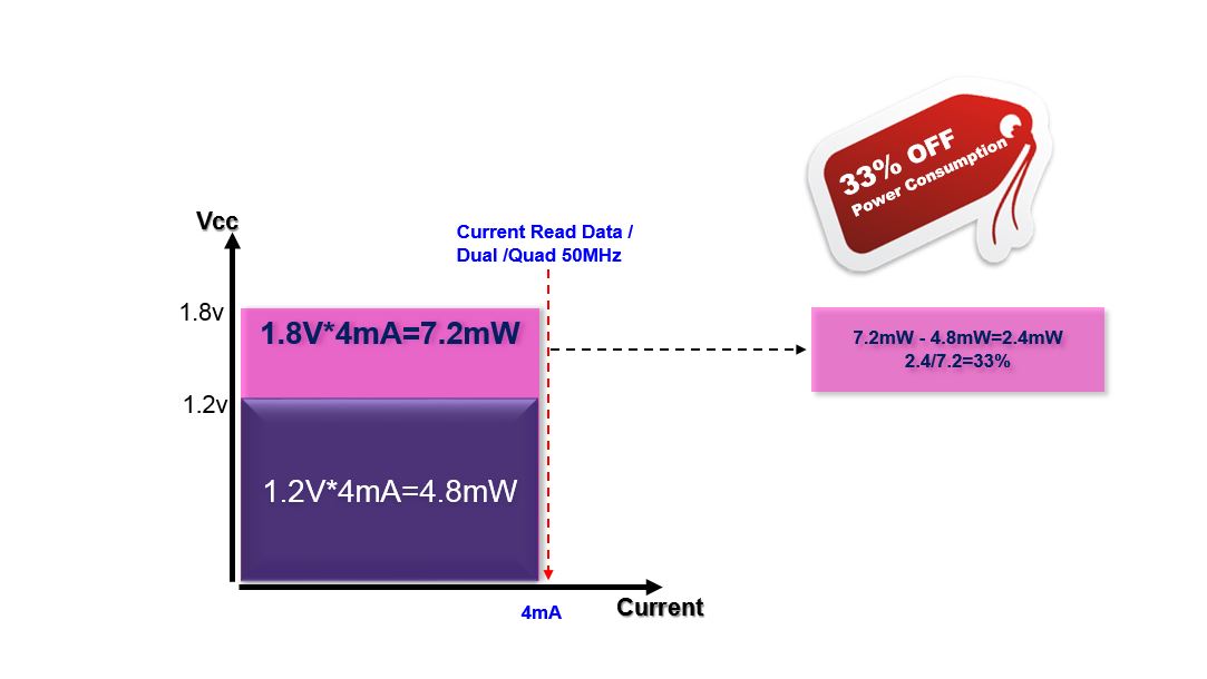
Figure 2 shows that the W25Q80NE, an 8Mbit NOR Flash IC operating from a 1.2V supply, offers a typical power saving in active mode of 33% over the equivalent 1.8V part.
Fig. 2: active power saving provided by 1.2V serial NOR Flash at 50MHz clock speed
Stand-by power is rated at <0.5µA in power-down mode. For comparison, power-down current is twice as high (<1µA) in Winbond’s 1.8V W25Q80EW device.
The reduced power usage in both active and stand-by modes offered by the W25QxxNE series enables system designers to increase battery run-time between charges, or to reduce the size and weight of the battery. But the new devices also provide additional advantages. First, the power circuit benefits from reduced noise coupling in the traces connecting the memory to the host SoC or processor, a direct result of the reduced power that they carry. This can help ease the requirement to implement noise mitigation measures such as shielding, and to improve the performance of noise-sensitive elements of the circuit.
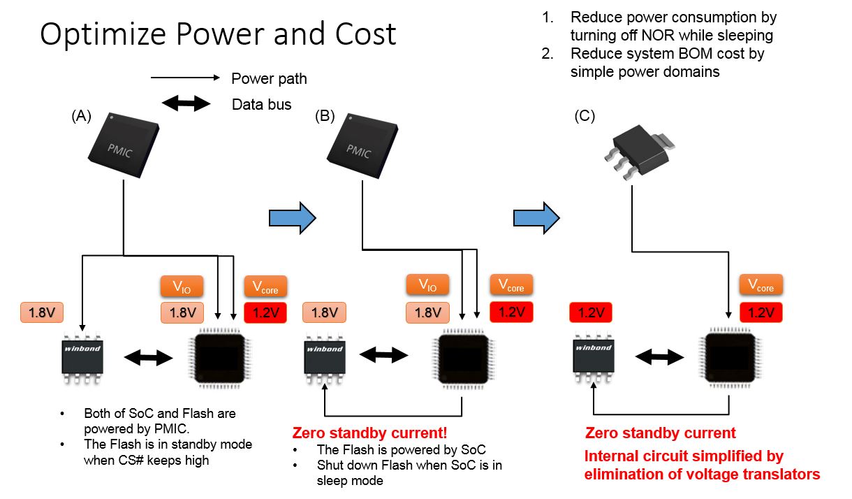
The other principal advantage of the 1.2V devices is the potential, over time, to simplify the power circuit (see Figure 3). As SoC, applications processor and microcontroller suppliers adopt the 1.2V power rail as standard, the requirement to support multiple power rails through use of a large, complex power management IC (PMIC) will disappear, freeing the system designer to use a simpler component such as a low dropout regulator (LDO) to provide a single 1.2V rail to the SoC. This offers the potential for substantial savings in board space and cost.
Fig. 3: replacing 1.8V Flash with 1.2V Flash can enable designers to simplify the power circuit
Feature set compatible with 1.8V devices
Winbond has designed the new 1.2V series and extended 1.5V series to match the existing 1.8V devices. In almost all respects, the W25QxxNE parts have the same features as the W25QxxEW parts, except that supply voltage, active power and stand-by power are lower. In addition, the maximum operating frequency of the 1.2V W25QxxNE series is 104MHz, the same as that of the 1.8V W25QxxEW. At 1.5V and 1.35V levels, the W25QxxND parts also operate at 104MHz; to enable the extended operating voltage range, their frequency at 1.2V is lower.
The 104MHz speed of the W25QxxNE and W25QxxND series is ample for typical applications in mobile, wearable and Internet of Things devices, since they support operation via standard, dual and quad Serial Peripheral Interface (SPI) and Quad Peripheral Interface (QPI), giving a maximum 52MB/s data transfer rate. This performance supports code shadowing to DRAM as well as Execute In Place (XIP) functions.
Because of the large size of Winbond’s product portfolio, and the wide choice of package styles that it offers, there is also considerable footprint compatibility between Winbond devices. The new 1.2V and extended 1.5V parts are supplied in 2mm x 3mm USON and a narrow 150mil 8-pin SOP. This SOP package is footprint-compatible with the popular WSON 6x5 package style used in Winbond’s 1.8V Flash devices.
Like the 1.8V serial Flash devices, the 1.2V and extended 1.5V serial Flash parts will support the same feature set and package types with minimal changes to the system software. This provides designers with the flexibility to use low-voltage and low-power serial Flash devices to simplify their power circuitry, with the additional benefit of saving power. The W25QxxNE 1.2V and W25QxxND extended 1.5V parts are also available in wafer and die form, as fully tested Known Good Die (KGD).
Momentum behind 1.2V and extended 1.5V power rails

Winbond has decided to be first to market in the serial Flash sector with 1.2V and extended 1.5V devices to give early momentum to a trend that seems certain to gain speed as manufacturers of battery-powered devices look for further savings in power consumption. The W25Q80NE 8Mbit 1.2V serial Flash part is available for sampling today and will be followed by the extended 1.5V 8Mbit W25Q80ND serial Flash part. Additional densities are well advanced on the development roadmap.

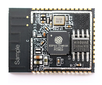
These 1.2V products have been designed in and endorsed by new chipset companies working in the low power area like Espressif, and here is what their CEO said. “Winbond’s low power serial flash products have been ideally positioned for IoT applications and smart connected devices,” said Teo Swee Ann, Espressif Systems’ CEO. “The Winbond 1.2V serial flash device pushes the envelope further and with our ultra low power ESP32 WiFi-Bluetooth combo chip, it has demonstrated its capability to help us further reduce power consumption; it has been tested successfully on our systems and we hope to bring this in the form of a module to the market as soon as possible.”
As a result, the Flash market is ready to standardise on 1.2V and extended 1.5V as the next power node below 1.8V, giving system designers the confidence to plan their development roadmaps around 1.2V as the supply voltage of the future.
By Conrado Canio, Technical Marketing Manager, William Chen, Product Manager and K. C. Shekar, Senior Director of Strategic Marketing, Winbond Electronics Corporation


