In March 2016, Google’s AlphaGo made history when it won a Go match with a 4:1 advantage, against Lee Sedol, an honorary 9 dan player from South Korea. Go, which originated in China over 3,000 years ago is a highly complex game that requires multiple layers of strategic thinking. Then, Google’s AlphaStar competed with two of the world's top gamers in "StartCraft II" at the end of 2018 and finally defeated the opponent with two 5:0 scores. Although as early as 1997, the computer program "Deep Blue" developed by IBM defeated the then chess grandmaster Garry Kasparov, but considering that the difficulty of playing chess is far lower than that of Go, AlphaGo's victory is to some extend regarded as "the real arrival of the AI era".

Origins of AI
From 1955 to 1956, John McCarthy, an assistant professor at Dartmouth College, was widely recognised as the father of artificial intelligence (AI). Marvin Minsky from Harvard University, Claude Shannon from IBM, and Nathaniel Rochester from Bell Labs in the United States jointly coined the concept of Artificial Intelligence (AI) saying "If machine can use different language to form abstractions or concepts, solve kinds of problems now reserved for humans, and improve themselves through autonomous learning, we call it AI."
The Oxford dictionary defines AI as ‘the theory and development of computer systems able to perform tasks normally requiring human intelligence, such as visual perception, speech recognition, decision-making, and translation between languages.’
As systems evolve, AI technology will be found in more IoT applications such as sensing, smartphones, network searches, face or vehicle license plate recognition, smart meters, industrial control and autonomous driving.

In the field of autonomous driving, level 4 testing (which is considered to be fully autonomous driving, although a human driver can still request control) has already been conducted in the United States. With Level 5 (true autonomous driving where the car does all the driving and there is no cockpit) autonomous driving is just around the corner, we will not only rely on traffic laws and regulations but also and the developers of the AI algorithms to ensure the safety of vehicles and pedestrians.
According to statistics from the International Data Corporation (IDC), the global AI services’ is expected to rise to 18.4% by 2024, with a market value of about $37.8 billion. This includes customised applications and related support and services for customised platforms, such as deep learning architectures, convolutional neural networks (a class of artificial neural network, most commonly applied to analyse visual imagery), AI-related chips (CPU, GPU, FPGA, TPU, ASIC) to name but a few.

IDC also predicts that global data storage will soar from 33ZB in 2018 to 175ZB in 2025, more than 50% of which will come from IoT devices.
Considering about 14 billion IoT devices will be deployed around the world by 2025, it is not of the utmost importance that we significantly increase the number of computing units and computing power in the cloud so as to cope with the massive data growth?
Well, the short answer is no. It does not consider the real challenges such as bandwidth and latency in the data transmission chain from endpoint to the cloud, which is why "edge computing" springs up so rapidly.
It is not necessary increase bandwidth and the number of servers to deal with the rapid increase of IoT devices. It is better to move applications to the endpoint devices so there is no need to send all of the data to the cloud for processing, transmission, storage, and analysis. For example, in an industrial automation application, data storage distance impacts efficiency - 5G mobile device manufacturers may experience serious battery life difficulties if they do not strengthen endpoint artificial intelligence and reform the computing-storage architecture.
Security is another important issue, especially in the Internet of Everything (IoE) era, where confidential information, data leaks or hacking incidents are common. Having computing happen at the edge minimises the number of times data is transferred in the "cloud-pipe-endpoint" path, in that case, power consumption and the total system cost of ownership is reduced while ensuring data and network security.
Comparing AI Chips
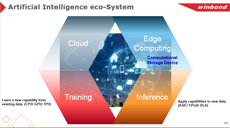
AI technology is divided into two categories; Training and Inference. Training is executed in the cloud by CPU, GPU, and TPU to continuously increase database resources for building data models. Inference relies on the trained data model and is more suitable for completing edge devices and specific applications. It is often processed by ASIC and FPGA chips.

AI-related chips include CPU, GPU, FPGA, TPU and, ASIC. To get an idea of how these chips compare to one another, here is a comparison focusing of 5 key factors. These are:
- Computing
- Flexibility
- Compatibility,
- Power
- Cost
- CPU
CPUs are developed with strong computing power and software and hardware compatibility that are second to none. But due to limitations of the von Neumann architecture, data needs to be transferred back and forth between the memory and the processor. This limits the average processing speed and the ability to push itself forward in power consumption and cost when compared to other solutions.
- GPU
Thanks to the adoption of the Compute Unified Device Architecture, Nvidia’s GPU, for example, can subjectively read the memory location and boost the computing power by sharing virtual memory. The average computing power exceeds CPUs hundreds or even thousands of times.
GPUs have developed with good software and hardware compatibility, but need improvement in power consumption and cost-efficiency. Investment in hardware such as additional cooling systems is also essential to reduce any heat issues.
- ASIC
ASIC chips are designed for specific applications. Their computing power, overall power consumption, and cost-efficiency can be optimised after verification and tuning.
- FPGA
FPGAs compatibility of software and hardware is commendable, even if the overall computing power, cost efficiency and power consumption are not the best. For developers, starting an AI chip development from a FPGA is still a good idea.
Breaking Through the Boundries of Von Neumann Architecture
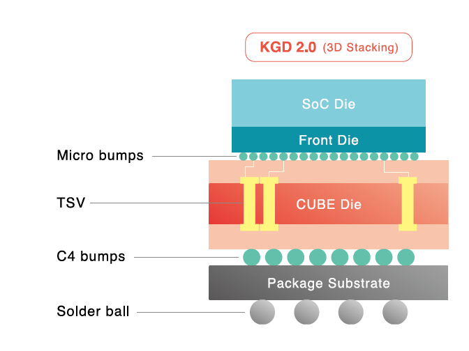
The von Neumann architecture which is widely adopted by traditional computing devices, does not separate computing and storage but focuses more on computing. The endless transmission of data between the processor and the memory consumes about 80% of the time and power. Academics have come up with many different ways to solve this - implementing high-bandwidth data communication through optical interconnection and 2.5D/3D stacking. Mitigating memory access delay and power consumption by increasing the number of cache layers and near-data storage such as high-density on-chip storage.
But is there any difference between computing and storage in the human brain? Do we use the left hemisphere for computing and the right one for storage? Obviously not. The computing and storage of the human brain happens in the same place with no data migration required.
Then, it is not surprising that both Academics and the Industry were eager to find a new architecture similar to the structure of the human brain with the ability to combine computing and storage organically. The solution was ‘Computational Storage Devices’, which computes using storage units directly or classify the computing units so they correspond to different storage units -minimising power the consumption caused by data migration.
Some manufacturers in the storage industry have explored different options. Non-volatile memory (NVM), for example, stores the analog signal generated by the digital-to-analog converter and outputs the computing power. Meanwhile, the input voltage and output current play the role of variable resistors in the NVM, and the analog current signal is converted into the digital signal by the analog-to-digital converter. This completes the conversion process from digital signal input to digital signal output. The biggest advantage of this approach is that it can fully utilise the mature 20/28nm CMOS process, instead of pursuing the expensive advanced process of 7nm/5nm like CPU/GPUs.
With the reduction of cost and power consumption, the delay has been significantly improved, which is crucial for applications such as drones, intelligent robots, autonomous driving, and security monitoring.
In general, the computational complexity of the endpoint inference process is low and the tasks involved are relatively fixed. With the low versatility requirements of the hardware acceleration functions, there is no need to frequently change the architecture. This is more suitable for the implementation of in-memory computing. Relevant statistics show that before 2017, artificial intelligence, whether training or reference, was completed in the cloud; but by 2023, AI reference on edge-side devices/chips will account for more than half of the market, with a total of $20-30 billion. This is a massive market for IC manufacturers.
What Kind of Flash does AI Require?
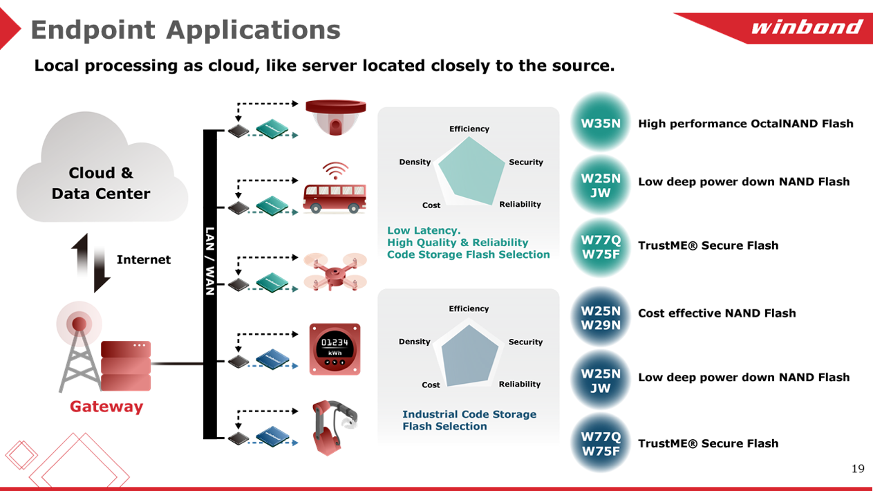
Everyone will agree how important high-quality, high-reliability and low-latency Flash Memory is for AI chips and applications. Finding the right balance of performance, power consumption, security, reliability, high efficiency for different applications is crucial. Cost, although important, should not be the most important consideration.
Winbond’s product portfolio, offers suitable options for AI applications including high-performance OctalNAND Flash W35N, the W25NJW series for low-power applications, and the security-related W77Q/W75F series of secure flash memory. The data transfer rate of Winbond QspiNAND Flash, for example, is about 83MB per second and the fastest speed of OctalNAND series is up to almost 3 times faster at almost 240MB per second.
Our AG1 125C NOR series and AG2+ 115C NAND series Flash are being mass-produced for automotive applications. Winbond also provides cost-efficient solutions such as the W25N/W29N NAND Flash series for line robot applications.

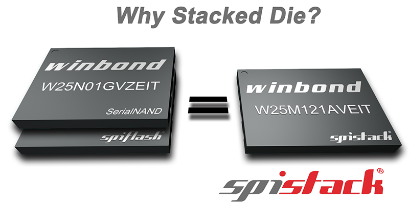
In addition to Winbond’s a wide range of Flash products, Winbond’s SpiStack (NOR+NAND) also offers a viable alternative. It stacks NOR and NAND dies into one package, such as 64MB Serial NOR and 1Gb QspiNAND die stack, offering designers the flexibility to store code on the NOR die and data on the NAND die. Although it is a stack of two dies (NOR+NAND), the single package of SpiStack only utilizes 6 signal pins.

"Winbond provides a variety of Flash options to protect the code model developed by customers. Just like in a basketball match, the chip manufacturer plays the centre or the forward, scoring with powerful computing power and algorithms; while Winbond, just like a defender, protects customers with high-quality, high-performance Flash products to ensure they keep scoring in the market." Comments Winbond.