Industry’s vision for the Internet of Things (IoT) foresees the installation of billions of devices connected to the world’s universal network. All forecasts for the numbers of IoT nodes are huge. Simple mathematical reasoning suggests that the average production cost per node must be small, otherwise the economics of the IoT simply are not viable. Most suppliers to the electronics industry are today working under the assumption that the bill-of-materials (BoM) cost of a node cannot exceed $5 on average.
The designers of these devices, then, are going to be under extreme cost pressure. Some IoT nodes, such as those used in homes or offices, will be able to take advantage of readily available Wi-Fi® or Bluetooth® wireless connectivity. These technologies, used so widely in consumer electronics, can be implemented cheaply in end nodes using off-the-shelf components.
Some applications however, including most that operate outdoors, will not be able to use a Wi-Fi or Bluetooth radio to link to an internet access point. Instead, many are likely to use other standard RF technologies which offer longer range than the 100m maximum typically available with Wi-Fi or Bluetooth connections.
Various technologies are available in the emerging category of low-power wide-area wireless networking (LPWAN): LoRaWAN, SIGFOX and NB-IoT have the best chance of achieving mass adoption in the view of most industry observers today. For these technologies, off-the-shelf, easy-to-use chipsets are either not available today, or are shipping in relatively low volume compared to the most popular Wi-Fi and Bluetooth Systems-on-Chip (SoCs).
So already the designer of an IoT node that connects to an LPWAN is facing a tough cost problem. And if the cost of the radio is relatively high, then the BoM budget available to the remaining components in the circuit is even smaller. Of these remaining components, the memory chips are among the most expensive, and so offer the greatest scope for cost optimisation.
This article explores the choices of memory architecture available to designers of IoT end nodes containing a LPWAN radio, and explains the advantages of various external Flash memory solutions, depending on the system’s requirement for performance, memory capacity and system size.
Typical application requirements
The configuration of internal and external memory capacity must be made in the light of the system’s functional requirements, which in turn depend on the application(s) it supports. The range of applications for LPWAN connectivity is of course huge. But examples of device types that might use LPWAN connections include:
- smart streetlights equipped with environmental sensors
- valuable portable assets used outdoors, such as temporary traffic signals or construction equipment
- farm machinery or even farm animals
In these examples, an SoC or microcontroller will be running application code as well as performing system management functions. This entails a requirement for memory: for code storage, for configuration data, and for user (application) data.
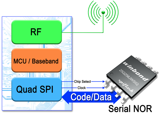
 Fig. 1: A low cost LPWAN SoC interfacing to a serial NOR Flash memory
In an application which puts a high emphasis on performance and is not constrained by a small BoM budget, a typical memory architecture for such a system would feature:
- a high-speed DRAM as scratchpad memory for the SoC
- Flash memory embedded in the SoC
- an external non-volatile memory IC, either a NOR Flash or NAND Flash device depending on the storage capacity requirement, for configuration data and user data
Driven by the demand for cost optimisation, however, IoT system designers are looking with increased interest at the different architectural options provided by the latest generation of external Flash memory devices. Figure 1 illustrates one such architecture: a LPWAN SoC with a Winbond 1.8V spiflash® device.
Higher-speed serial Flash
Designers of cost-sensitive IoT nodes can benefit from the availability of serial Flash devices that offer very high data-transfer rates, and use them to implement an architecture different from the conventional model. The high speed of today’s serial Flash memories gives designers of IoT nodes the ability, in almost all cases, to eliminate the DRAM scratchpad memory and to use a low-cost SoC that has minimal internal Flash capacity. Such a Flash-based architecture reduces component count, system size and BoM cost while maintaining the performance required by the application.
That serial Flash should be capable of providing sufficiently high data-transfer rates to replace DRAM is on the face of it rather surprising. After all, the main benefit of serial Flash is that it can provide reliable non-volatile storage capacity with a very low pin count and a small package – but the low pin count should in theory also entail low bandwidth. The opposite is true of parallel Flash: it provides numerous channels for very high bandwidth and data rates, but in order to do so a parallel Flash IC has many pins, and therefore a system using parallel Flash has a large and complicated board footprint.
Manufacturers of serial Flash, however, have over time developed ways to square the circle, increasing the data-transfer rate while maintaining small package outlines with a low pin count. Now, serial Flash devices featuring Quad Serial Peripheral Interface (QSPI) or Quad Peripheral Interface (QPI) technologies and operating at speeds as high as 133MHz can boast maximum data rates of as much as 66MBytes/s. This is sufficient to support Executive-in-Place (XiP) functionality, in which an SoC or processor executes application code directly from the external Flash memory without shadowing it to DRAM, enabling the elimination of the DRAM device entirely. Fast serial Flash with QSPI or QPI capability can also implement pseudo-cache execution for frequently executed functions to boost performance.
A serial Flash device can meet all the system’s storage needs: its memory address range can be divided into separate sections for code and for data. Firmware is stored in the code section, while the data section contains user data and configuration settings.
Since information stored in the data section is continually being erased and replaced with new data, this section has to support a high number of program/erase cycles. Of the two types of serial Flash – NOR Flash and NAND Flash – NOR is inherently the more robust technology, and can reliably be operated without the need for Error Correction Code (ECC). All serial NOR Flash devices supplied by Winbond are rated for a minimum of 100,000 program/erase cycles.
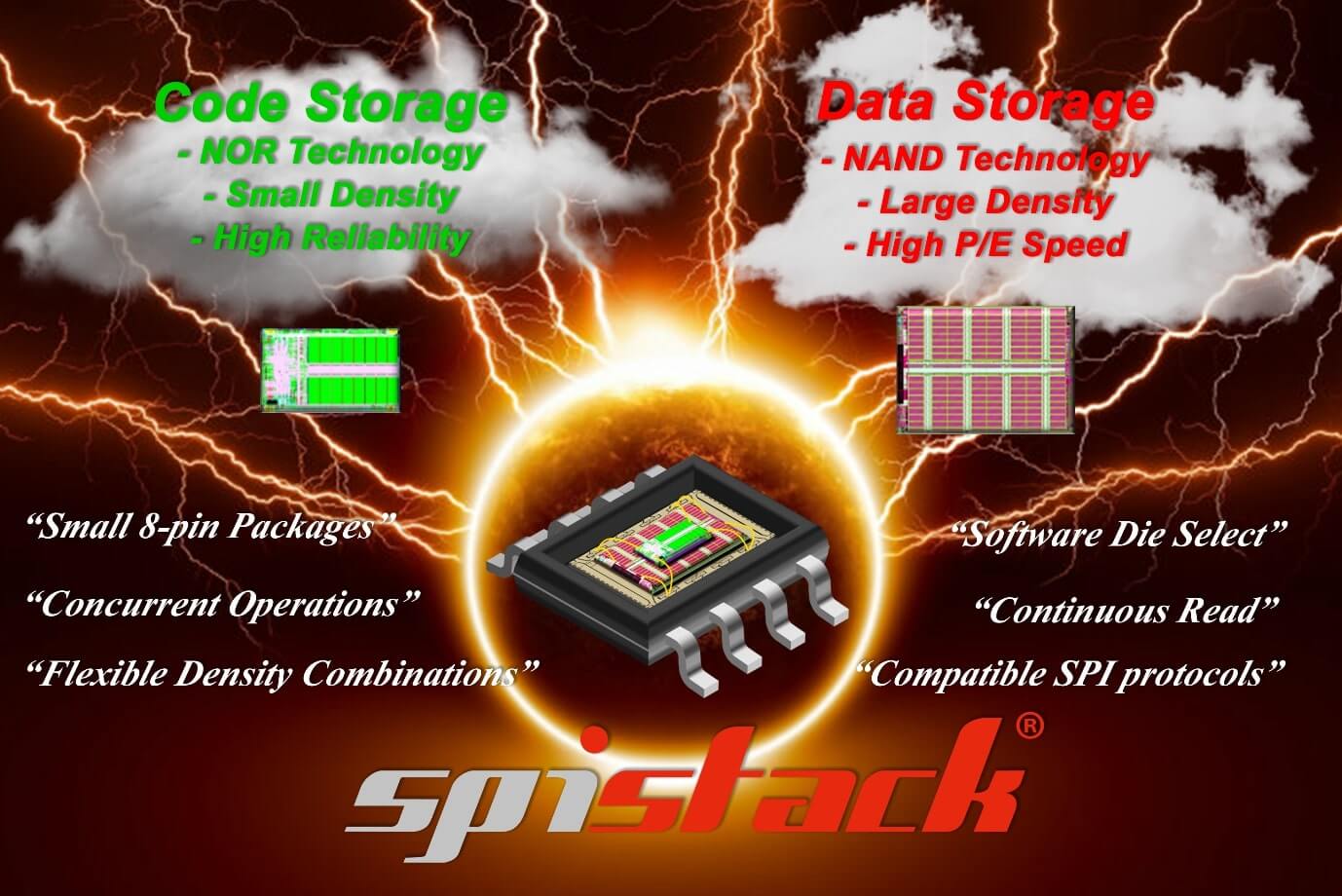
 Fig. 2: a serial NOR Flash die may be co-packaged with a QspiNAND Flash die in a SpiStack product. (Image credit: Winbond)
For applications requiring a total Flash memory capacity of less than 512Mbits, normally the most cost-effective option is serial NOR Flash. At a memory density of 512Mbits or more, QspiNAND Flash normally becomes the cheaper option. All NAND Flash memory requires a controller to manage its operation, including detecting and correcting errors in random memory locations, managing blocks of memory that have errors in them (bad block management), and relocating or mapping locations with errors to new locations that are error-free.
Winbond’s QspiNAND Flash products, available in 512Mbit, 1Gbit and 2Gbit densities, contain features which reduce the number of tasks that an external NAND controller has to perform. These include an internal ECC and a bad block management function. Winbond NAND Flash provides an internal 1-bit ECC for each 528 bytes of memory. Winbond QspiNAND with 1-bit ECC is rated for a minimum 100,000 program/erase cycles.
The QspiNAND Flash internal bad block management allows a read access to a bad block to be automatically re-mapped to a good block according to settings in the internal look-up table (LUT). The LUT can have up to 20 links. This bad block access re-mapping via LUT allows continuous read operations across pages and the full memory range that mimics serial NOR functionality. This is unlike QspiNAND products offered by other vendors that only offer limited Page Read access, providing slower read throughput performance.
A third option available to the designer of an IoT gateway is a combination of Flash memory dies in a single stacked package, available from Winbond in its SpiStack® product (see Figure 2). The SpiStack can be configured flexibly, to combine two or more NOR Flash dies, two or more NAND Flash dies, or a NOR die with a NAND die. A typical SpiStack configuration consists of a serial NOR Flash die for highly reliable code storage combined with a QspiNAND Flash die for data storage, in a single 8-pin WSON package measuring 8mm x 6mm. This solution offers the advantage of flexible Flash memory options/capacity while maintaining a low pin count: a SpiStack device has a single 8-pin package and a single Chip Select pin. The provision of a single Chip Select pin is enabled by Winbond’s software die selection ‘C2h’ instruction for selecting the active die.
The memory densities available in serial NOR, QspiNAND and SpiStack products are sufficient to meet the needs of IoT nodes connecting via an LPWAN. LoRaWAN nodes, for instance, typically require serial NOR Flash at lower densities up to 16Mbits, operating at either 3V or 1.8V. Nodes connecting via NB-IoT will generally need higher serial NOR Flash densities in the range 32Mbit to 128Mbit, and operating at the lower 1.8V level, although some applications might need a much larger data capacity of 1Gbit or more, in which case they will need a QspiNAND Flash or SpiStack memory.
IoT nodes using LPWAN connectivity are mobile and many of them are battery-powered, and so power consumption is a prime concern of the system designer. Serial Flash ICs are available as standard from any supplier with 3V or 1.8V ratings, of which the 1.8V version offers lower consumption in active and stand-by modes.
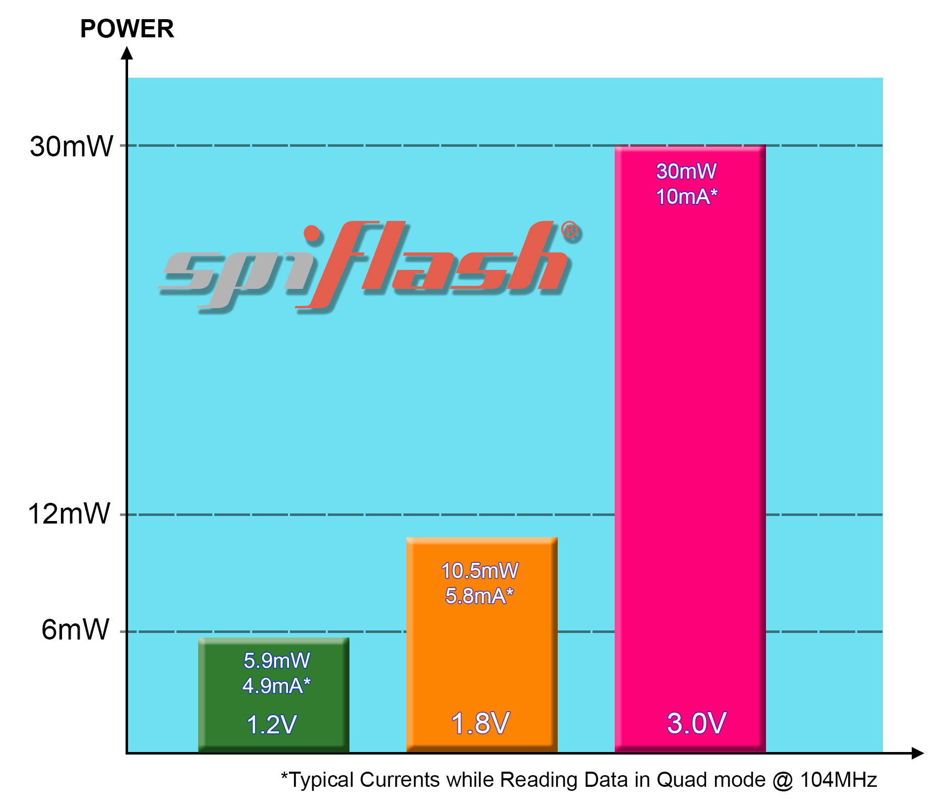
Fig. 3: Winbond serial NOR Flash ICs Active Read current performance ratings, including in green new 1.2V parts. (Image credit: Winbond)
In June 2017, Winbond also introduced a new ultra-low power range of serial NOR Flash ICs (see Figure 3). The new 1.2V products cover an operating voltage range from 1.14V to 1.3V, while the 1.5V devices have a wider operating voltage range from 1.14V to 1.6V, giving portable designs the advantage of sustained battery operation, both when the battery is fresh and when its voltage decreases over use or time. The new low-voltage parts, available in densities from 1Mbit to 128Mbits, can draw as little as 4.9mA in active mode at 104MHz, and just 0.5µA in power-down mode.
Cost and space savings with high-speed serial Flash
Designers can, then, save space and reduce component count and cost by configuring a DRAM-less design that uses high-speed QSPI or QPI serial Flash and implements XiP. Further space savings are available with the use of a stacked-die product such as SpiStack, and new 1.2V and 1.5V serial NOR Flash devices lower power consumption in mobile, battery-powered applications.
Thus the latest generation of serial Flash products enables the designer of IoT nodes connected via LPWAN to meet their performance requirements while offering component cost reductions that help achieve the tight target of $5 for total system BoM cost.
By Conrado Canio, Technical Marketing Manager, Winbond Electronics Corporation America
More information please visit Winbond Electronics Corporation.