The direction and force of consumer demand is relentless: buyers of mobile and computing devices are constantly looking for products that offer more features and better performance in a smaller, lighter, sleeker form factor. Applications that once would have required a laptop have migrated to the smartphone. Now smart watches are supporting applications that were previously performed only on smartphones.
When product designers are evaluating new ways to meet this constant demand for miniaturization, system storage is one of their top priorities: serial NOR Flash memory (typically used for storing code) and QspiNAND Flash memory (typically used for data storage and as a back-up location for code) occupy a relatively large proportion of the total board real estate in many space-constrained designs.
Winbond, which produces around 30% of the world’s serial NOR and QspiNAND Flash ICs has previously helped to address this problem through its invention of the Quad Serial Peripheral Interface (QSPI) – a high-bandwidth version of the standard serial peripheral interface that enables very high-speed Read/Write operations to take place between a Flash memory and a host System-on-Chip (SoC), microprocessor or microcontroller. Supporting data rates comparable to those achievable with parallel Flash but using far fewer channels and smaller packages, Winbond’s QSPI innovation was an important step in the miniaturization of the memory system’s board footprint.
But more recently serial Flash manufacturers have adopted an additional way to increase memory capacity while reducing footprint: stacking Flash memory dies inside a single package.
This article outlines the impacts of replacing two or more discrete Flash memory ICs with a single stacked-die package, and describes a new approach to die stacking developed by Winbond that gives improved performance and a reduction in pin count and board footprint compared to alternative solutions.
The benefits of stacking memory dies
A typical Flash memory use case in a small device design might consist of a 16Mbit serial NOR Flash device for code storage, and a 1Gbit QspiNAND Flash device for data and a Linux® operating system. NOR Flash offers superior random access performance and excellent endurance and retention, important features for storing code that is read very frequently. NAND Flash offers faster programming, and is markedly cheaper than NOR Flash at densities greater than 512Mbits. Latency in Read operations is longer, but this is acceptable for data that is infrequently accessed.
Typically, then, system designs today have to accommodate on the board two Flash memory packages, each with its own interface to an SoC.
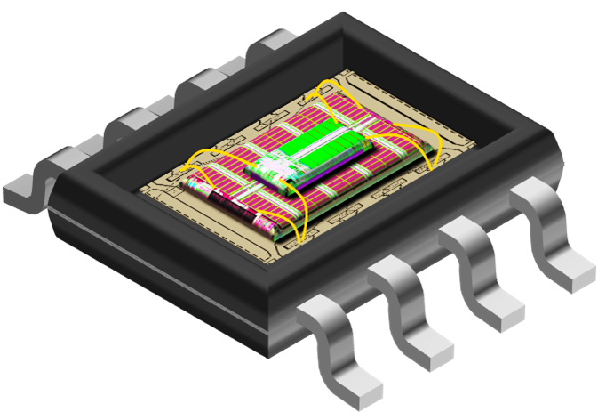
In this use case, the use of a stacked-die package offers an immediate reduction in board footprint (see Figure 1). In a heterogeneous package, a smaller NOR Flash die may be stacked on top of a larger NAND Flash die.


Fig. 1: a smaller NOR Flash die is stacked on top of a larger NAND Flash die. The dies and bond wires may be mounted to a leadframe or substrate. (Image credit: Winbond)
It is equally possible to benefit from the use of a homogeneous stacked solution, in which a NOR die is stacked on a NOR die or a NAND on a NAND. For instance, if an existing product design using a 512Mbit NAND Flash IC requires additional data storage capacity, the conventional approach would be to replace the 512Mbit IC with a 1Gbit device. But if the 1Gbit device has a different footprint and pin-out, this change will entail some time-consuming board re-design.
A homogeneous stacked package can eliminate the need for a board re-design: a 512Mbit die stacked on top of a 512Mbit die can be housed in the same package with the same pin-out as the single-die 512Mbit IC, allowing the designer to double memory capacity instantly with no requirement for a board re-spin.
These benefits – reduced board footprint and reduced development effort – are inherent to any implementation of the stacked-die concept.
But now Winbond has introduced a new approach to the stacking of Flash dies which provides an even greater reduction in board footprint while also offering improved Read/Write performance.
Low pin-count stacking
One of the main challenges in implementing a stacked-die product is the provision of interfaces between the SoC or microcontroller and the two (or more) dies inside the Flash memory package. To avoid contention on the SPI bus, the SoC uses a Chip Select (CS) command which tells the stacked package which die it wishes to interface to.
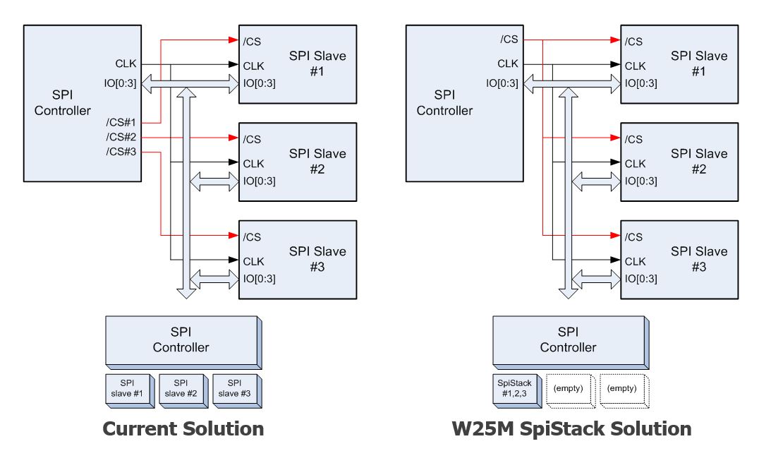
In other stacked memory solutions, this CS function is implemented in hardware over dedicated CS lines – one CS line to each die. So in a package containing two dies, there will be two CS lines, for three dies there are three CS lines and so on.
Clearly this has the unfortunate effect both of requiring more pins on the memory device and on the SoC, and more traces on the board.
Fig. 2: implementing the Chip Select function in software requires only one CS pin. (Image credit: Winbond)
In the latest W25M SpiStack® Flash memory products from Winbond, this problem is solved by use of a software Chip Select function which operates over a single CS channel between the memory device and the SoC (see Figure 2). Each die in a SpiStack package has a unique ID, and a simple Chip Select command using the relevant ID tells all the dies in the package which one is to occupy the SPI bus.
This software CS function operates via just a single CS pin on the memory device and on the SoC, and requires only one board trace between them. This reduction in pin count enables Winbond to accommodate two, three or even four dies in a standard 8-pin SOP or 8-pad SON package, whereas other stacked-die implementations using a hardware CS function typically use 16-pin SOP or 24-ball BGA packages which entail a much larger and more complex board design (see Figure 3).


Fig. 3: multiple dies in a SpiStack device may be accommodated in an 8-pin package. (Image credit: Winbond)
It is easy for the designer to integrate the SpiStack CS function into system software. The C2h command is used to select any die in the Flash memory package (see Figure 4). It can be issued at any time to change the active die, regardless of its operating status. Only one selected die is active on the SPI bus at any one time.


Fig. 4: the C2h Chip Select command uses a unique ID for each die in a SpiStack multi-chip package. (Image credit: Winbond)
Faster Read/Write operations
It is an inherent attribute of Flash memory technology that programming operations are relatively slow by comparison with other technologies such as SRAM and DRAM. When using a single-die Flash IC, then, it often happens that the system needs to read from memory while a long Write operation is still in progress. The controller then has to issue a command to suspend writing, read out from the memory, and then issue another command to resume writing. This makes use of the Flash device complex, and slows both the Read and Write operations.
Winbond’s introduction of a new concurrent operation feature in its SpiStack products removes this bottleneck. Put simply, concurrent operation enables the SoC to maintain Write or Erase operations on one die in a SpiStack product while reading from another die (see Figure 5).


Fig. 5: in a two-die SpiStack device, one die can occupy the SPI bus while another performs program or erase functions. (Image credit: Winbond)
As we saw above, only one die can access the SPI bus at any one time. But a SpiStack device can concurrently read while programming, read while erasing, program while erasing or program or erase on multiple dies simultaneously.
In many applications, this support for concurrent memory operations provides for substantial increases in operating speeds. It means that a SpiStack device has the potential to operate faster than any comparable device operating in sequential mode only.
Many homogeneous and heterogeneous choices
SpiStack multi-die packages are available in a wide variety of package types and densities, in both heterogeneous (NOR + NAND) and homogeneous (NOR + NOR, NAND + NAND) configurations. An advantage of Winbond’s position as the world’s biggest manufacturer of serial Flash is that it provides system designers with the widest choice of memory densities and package options.
Users therefore enjoy considerable design flexibility, benefiting from the freedom to swap devices with a common footprint and pin-out to meet changing memory density requirements.
SpiStack devices available today include:
- a 16Mbit NOR + 1Gbit NAND
- a 512Mbit NOR consisting of two 256Mbit NOR dies
- a 2Gbit NAND consisting of two 1Gbit NAND dies
Winbond’s SpiStack roadmap shows many other options becoming available during 2017, or on customer request.
By K. C. Shekar, Senior Director of Strategic Marketing and Takehiro Kaminaga, Assistant Professional Manager Winbond Electronics Corporation
For more product information, please visit Winbond SpiStack Flash

