Automotive displays, both in the instrument cluster and in the Centre Information Display (CID), or head unit, are becoming larger, more sophisticated and more numerous. Thanks to the popularity of devices such as tablets and smartphones, car users have grown accustomed to interacting with technology via colourful graphics rendered on large, high-resolution displays.
Car makers are responding to this changing consumer trend already by integrating displays of 7” size and above in the CID. Over time, the trend to a more graphical style of user interface is expected to see three or even more displays mounted around the driver, in the style of an aircraft’s cockpit.
The same trend is in evidence in the instrument cluster. New mid-range vehicles today will typically feature a hybrid design combining mechanical dials with a medium-sized 2D graphics display. At the high end, the traditional instrument cluster has now been superseded by large displays in which dials are rendered digitally as graphics, and driver assistance, navigation and infotainment graphics are displayed alongside the virtual dials (see Figure 1).
This dramatic change to the automotive user interface is helping to modernise both the appearance of the car’s interior and the driver’s user experience. But it also calls for a rethink of the specification of memory devices in infotainment systems.
The new, graphics-rich display systems run on a much larger code base than smaller, simpler displays, and the display system also handles much larger quantities of data in automotive display applications such as mapping and navigation or the various types of Advanced Driver Assistance Systems (ADAS). In the past, automotive display systems have normally used a NOR Flash chip for non-volatile code and data storage, a device type which is highly reliable and supports high-speed Read operation – two attributes which are highly prized by automotive system designers.
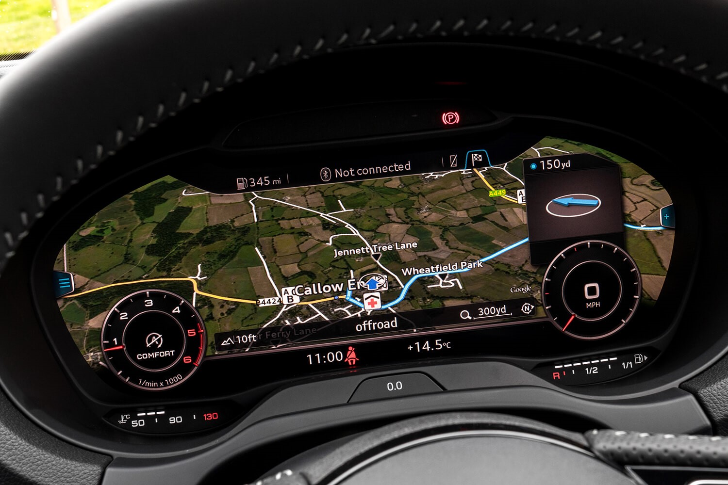
Fig. 1: the Audi Virtual Cockpit, an example of the new graphics-rich digital instrument cluster. (Image credit: Audi)
NOR Flash is a relatively low-density memory technology, however: for code storage requirements above 512Mbits, economic factors weigh heavily against NOR Flash. In high-end vehicles, car-makers have looked to borrow from the consumer electronics world, adopting the eMMC solid-state memory technology which is widely used in smartphones and laptop computers. But many automotive designers will have valid cost and reliability concerns over the use of eMMC storage devices in low-end and mid-range vehicles.
This leaves a gap for another memory option: a serial NAND Flash product newly developed by Winbond. But NOR Flash has always in the past been preferred to NAND Flash in automotive storage applications. Has enough changed to make a new NAND device acceptable for use alongside automotive displays?
The Automotive Display System Requirements: Speed, Reliability and Compatibility
In automotive display system development, storage devices have to meet three important requirements.
First, they need to provide a high Read speed. This is because car makers set a target of booting up display and infotainment systems in a maximum of one second, for the convenience of the user. The normal architecture involves code shadowing from a non-volatile Flash storage device to a DRAM main memory, from which the code is loaded into the host SoC. If a large quantity of code is to be loaded to the SoC and executed in less than one second, it follows that the Read speed from the Flash device must be high. This is a strength of SPI NOR Flash products such as the SpiFlash® range from Winbond, which offer a maximum Read speed of 50Mbytes/s.
Second, all automotive systems must be highly reliable: buyers expect vehicles to provide a long operating life of at least ten years, and reliability rankings and car makers’ brand values are heavily dependent on consumers’ perception of vehicles’ reliability.
In non-volatile storage, reliability is affected by two main factors:
- Bit errors, which can occur during both Read and Write operations. The operation of NOR Flash technology produces negligible levels of bit errors, and these bit errors can be corrected through the implementation of 1-bit Error Correction Code (ECC).
- Electron leakage from Flash memory cells can result in loss of data after a period of time, creating potential read errors. Operation at extreme high temperature has the effect of accelerating electron leakage and thus shortening the average duration of data retention across a Flash device’s cells. Data retention is very good in NOR Flash memory chips, because of the relatively large size of the memory cells, which means that each cell contains a large number of electrons.
The third key requirement for a data storage chip in automotive systems is compatibility with legacy designs. Automotive system development is normally a matter of evolution rather than revolution. The high cost of qualifying and validating new hardware and software components tends to encourage design teams to extend performance or add new features by building on an existing code base that runs on a familiar SoC architecture.
These three factors have all counted in favour of NOR Flash as the preferred non-volatile memory technology for the instrument cluster and automotive displays. It offers high data transfer rates, low bit error rates, long data retention, and well understood protocols governing the interface to the host SoC.
The use of NOR Flash in automotive displays, however, is now in question. As stated above, the low density and large cell size of NOR Flash confers an advantage in terms of data retention. But it also means that the die size, and therefore the cost, of the chip rises quickly as storage capacity increases. NAND Flash technology has a much smaller cell size: this higher memory density means that NAND Flash memory is a cheaper option for larger data capacities.
In fact, the cost-per-bit of a serial NAND Flash IC is typically less than half that of the equivalent SPI NOR Flash solution at densities of 512Mbits and more – exactly the densities that will be required for the new, larger automotive displays.
In the past, however, automotive designers would have resisted the suggestion that they should embed a NAND Flash IC in infotainment systems, in which speed and reliability are of such critical importance. In consumer electronics devices such as mobile phones, NAND Flash memory is used for storing user data such as music and photos. But the assumption in the automotive community has been that NAND Flash ICs offer too slow a data transfer rate, are prone to high bit error rates and suffer from limited data retention particularly at the elevated temperatures commonly experienced in automotive applications.
This may be true of the low-cost, ultra-high density NAND Flash ICs used in multimedia consumer devices, chips which are fabricated at advanced process nodes below 20nm.
But a high-performance serial NAND Flash design newly developed by Winbond succeeds in combining high density and low cost-per-bit with the speed and reliability that automotive developers require.
New High Performance QspiNAND Flash
The new 1Gbit W25N01JW is a single-level cell (SLC) serial NAND Flash IC built using Winbond’s proprietary 46nm fabrication process. SLC NAND Flash has a larger cell size than the higher-density multi-level cell (MLC) and triple-level cell (TLC) NAND types used in consumer electronics. This larger cell size and the relatively large 46nm circuit features mean that electron leakage does not compromise data retention.
The W25N01JW device retains data for 10 years at a continuous 70°C after 10,000 Program/Erase cycles (see Figure 2). This is in sharp contrast to the performance of eMMC devices, which are today widely used for data storage in the CIDs of high-end vehicles, and which retain data for a fraction of this time even when used in SLC mode.
The W25N01JW also implements 1-bit ECC on all Read and Write operations to correct all 1-bit errors, and complies with the endurance, retention and quality requirements of the AEC-Q100 standard and relevant JEDEC specifications.
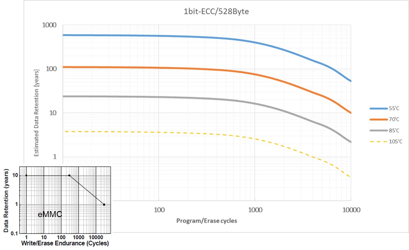
Fig. 2: data retention of the W25N01JW (main diagram) and of a typical eMMC device (bottom left). (Image credit: Winbond)
In the W25N01JW, Winbond has also introduced innovations which produce the highest ever data transfer rates in a NAND Flash memory: 83Mbytes/s via a Quad Serial Peripheral Interface (QSPI), matching the read speed of today’s automotive SPI NOR Flash. The new Winbond architecture also supports a two-chip dual-quad interface which gives a maximum data transfer rate of 166Mbytes/s (see Figure 3).

Fig. 3: the two methods for implementing the dual quad I/O interface in Winbond’s new high-performance serial NAND Flash architecture. (Image credit: Winbond)
The SoCs which control next-generation ADAS and instrument clusters stream data on the data bus at a maximum rate of around 200Mbytes/s. This means that Winbond's high-performance serial NAND Flash in dual or quad I/O mode can support 80% of this data flow.
The new high-performance serial NAND from Winbond, then, meets the speed and reliability requirements of automotive designers, at a markedly lower cost than SPI NOR Flash at densities of 1Gbit and more. It also meets the third test for alternative memory solutions: compatibility.
The W25N01JW is supplied in WSON and TFBGA packages with a standard 8mm x 6mm footprint shared with NOR Flash ICs. It also supports a NOR Flash-compatible protocol as well as the standard serial NAND protocol, so that automotive system designers can replace NOR Flash in an existing design with Winbond’s high-performance serial NAND without having to rewrite the application’s code.
Ready Availability of a Superior NAND Flash Technology
Winbond's high-performance serial NAND Flash technology offers both cost and performance advantages over the SPI NOR Flash typically used today in the instrument cluster and in automotive display systems. In addition, Winbond has in-house fabrication capacity and full control over the manufacturing process, and so can guarantee a long-term steady supply to automotive customers.
By Takehiro Kaminaga, Flash Memory Marketing Manager, Winbond Electronics Corp. Japan
A Deputy General Manager who works at the Flash Memory department Marketing and FAE group for Winbond Electronics Corporation Japan. In 2010, he joined Winbond and was responsible for NAND product planning and promotion. Prior to joining Winbond, he served as Marketing Manager in Eterna memory, and served as Marketing Manager in Vantel. He has over 19 years of experience in memory related field.


 English

