SPI NOR Flash is the electronics design engineer’s favourite memory type for low-density, high-reliability storage of application code and data in embedded systems with a storage requirement of up to 512Mbits.
To facilitate broad adoption across the industry, NOR Flash memory technology follows certain standards, for instance governing the serial interface to a host microcontroller or SoC. One of these standard features is the way in which NOR Flash allows the system designer to configure protection of stored data. Protection may be applied to a specified fraction of the entire memory array in which mission-critical data is stored: most often, this is boot code, since if boot code were impaired or lost, the entire system would be disabled.
Protection helps to ensure that data in protected blocks is not corrupted, for instance by noise, or mistakenly erased and overwritten by a faulty operation implemented by the host system. If an Erase or Program command specifies a memory region that contains a protected block, this command will be ignored. In other words, protected blocks are tagged as Read-only memory.
The way in which the standard approach to data protection was implemented many years ago in NOR Flash has more recently, however, begun to constrain designers’ flexibility in their use of the higher-density memory devices available today. This has prompted Winbond to introduce new, proprietary extensions to the standard protection functions to give more control over the block size and the operation of the protection function. This article describes the reason for introducing these new features, and outlines their uses for system designers who use NOR Flash memory.
Increase in protected block sizes
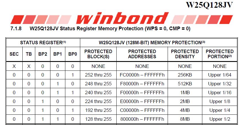
When the data protection function was created many years ago, NOR Flash memory densities were much smaller than they are today. At that time, just three Block Protection (BP) bits in the Flash IC’s status register were enough to specify the portion of the total memory array that needed to be protected. In a Winbond NOR Flash memory device’s datasheet, these status register bits are shown as BP0, BP1 and BP2. These three bits give eight options for selecting the size of the protected region, from as little as 1/64th of the array to as much as ½ (see Figure 1).
Fig. 1: the BPx bits in the status register of a NOR Flash device allow the user to specify the size of the protected region. (Source: Winbond W25Q128JV datasheet)
So the maximum granularity available to the user is 1/64th of the total array. The problem today is that embedded systems require more storage than before, and Flash memory manufacturers have responded by providing products with larger memory capacity. The Winbond W25Q128JV, for instance, is a 128Mbit memory: a 1/64th portion is 2Mbits. But what if the system designer only needs to apply protection to boot code, and not to any other code or data? And the boot code is just 50kbits?
In this case, a protected region of 2Mbits would store just 50kbits of code, and so – because the region has Program and Erase protection – most of the protected block will remain empty.
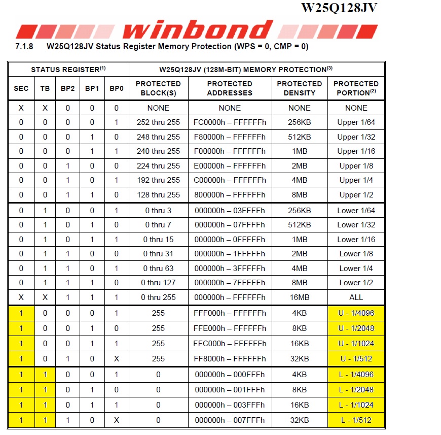
Now Winbond has introduced a new feature to solve this problem: it is the ‘SEC’ status register bit shown at the far left in Figure 1. This SEC bit allows the designer to specify protection at the sector rather than the block level. As Figure 2 shows, this divides the array into portions as small as 1/4096th – 32kbits in the W25Q128JV part, for instance. This gives the designer the flexibility to protect very small pieces of critical code, such as boot code, while leaving almost all of the memory array free of Program/Erase protection and available for storage of any other code and data.
Fig. 2: the SEC register bit enables protection to be specified at the sector level. (Source: Winbond W25Q128JV datasheet)
Figure 2 also shows, highlighted in yellow, another feature introduced by Winbond: the TB (Top/Bottom) register bit. By default (TB=0), the allocation of block or sector protection starts at the bottom of the memory array of addresses. This is because most CPUs boot from the bottom of the array, so the protected region holding boot code should be located at the bottom for the fastest operation and the most efficient use of main memory.
Intel CPUs, however, boot from the top. So with the TB bit, Winbond gives users of Intel devices the option to allocate memory addresses at the top of the array for block or sector protection, by configuring TB=1 in the status register.
Applying block protection to almost an entire array
In standard NOR Flash memory ICs, the option to configure blocks for Program/Erase protection starts with the smallest 1/64th increment, and enables protection for up to half of the array, as shown in Figure 2. In some applications, however, the requirement for storage of user data is nil or almost nil, and nearly all the memory array is occupied by boot and fixed application code. An example of such an application is a TV remote control: here, only a small amount of unprotected memory space is required for infrequent end-user configuration settings (for instance to pair the remote control to a new media device). Nearly all the memory space is for application code, which will not change and so benefits from Program/Erase protection.
A status register bit provided by Winbond meets this application requirement. It is the Complement (CMP) bit: this reverses the protection setting asserted by the BP and SEC bits. If the BP bits are configured to protect a 1/64th portion of the memory array with the default setting of CMP=0, when CMP=1 protection will be applied to a 63/64th portion of the array, and only 1/64th will remain unprotected.
Reinforced protection with hardware lock on status register settings
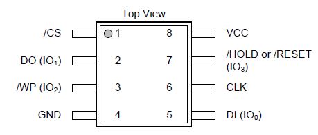
To provide additional confidence in the protection of critical data such as boot code, a NOR Flash memory IC can apply a hardware lock to the block/sector protection firmware (register) settings. This is achieved via the WP pin (see Figure 3). The status of the WP pin is controlled with the SRP (Status Register Protect) register bit.
Fig. 3: pin assignments on the W25Q128JV SOIC package, showing the Write Protect (WP) pin. (Source: W25Q128JV datasheet)
Some users might be familiar with the WP pin in parallel Flash devices, which has a simple Write Protect function. The function of the WP pin in serial NOR Flash devices is different: it protects the register settings that configure the Program/Erase protection of blocks and sectors via the BP and SEC register bits. Once the BP and SEC settings are made and the WP pin is asserted (WP=Low), no change to the BP and SEC settings may be made without pulling the WP pin High.
The ultimate protection of critical data
Users of serial NOR Flash devices such as the Winbond SpiFlash® series of products can guarantee that protected regions will never be programmed or erased after shipment from the factory – effectively turning protected blocks into one-time programmable (OTP) memory space.
This is achieved by applying a permanent lock to the block and sector protection register settings. The so called Active Permanent Lock can be applied with the SRL (Status Register Lock) register bit. This permanently, irrevocably locks the data in protected blocks. If a bug is found in protected code in future, or an important security update needs to be applied in the field, it cannot be done if the Active Permanent Lock has been implemented. This is a serious consequence, and so Winbond requires a special instruction sequence to be followed to implement Active Permanent Lock, which is only available by application to Winbond – the instructions are not listed in the datasheet.
For most users, a better option is the Power Supply Lock-Down function: this has the same effect of locking the status register settings when the device is active, but each time the device is powered down the status register lock is lifted. This leaves a window open to change the register settings every time the device is powered on before the Power Supply Lock-Down is implemented again.
Enhanced data protection with advanced Flash features
This article has described a number of features of the operation of SpiFlash NOR Flash memories from Winbond which may be used to protect critical data. These protection features help designers to avoid the risk that their system will be disabled because of bit errors caused by noise, or because a host SoC mistakenly overwrites critical data.
The range of options for protecting data, and for locking the protection settings, is not necessarily well known even by long-standing users of NOR Flash memory devices. System designers can take advantage of them to improve the reliability of their products’ field operation, simply by using the full array of register settings provided by Winbond in SpiFlash NOR Flash devices.
Please contact mkt_online@winbond.com if you have any further questions.
by Ken Lin, Deputy Director of Flash Memory Technical Marketing and Application Engineering, Winbond Electronics Corporation


