The potential for innovation created by artificial intelligence (AI) is exciting embedded developers in every market sector. In fact, it might seem strange to be thinking in terms of ‘innovation’, since the fundamental technology of AI is not itself new: IBM’s Deep Blue AI system beat chess world champion Garry Kasparov as long ago as 1997.
But for two decades after this early breakthrough, progress in introducing AI technologies was slow. It was only in the late 2010s that the constellations aligned in such a way as to bring AI into the mainstream of embedded development, the path smoothed by two factors: first, the availability of huge training data sets, generated by sensor-rich IoT systems. Large collections of tagged images, video and other forms of data are also available for the first time because of the popularity of platforms such as YouTube, Instagram, Snapchat and Facebook Live.
Second, the capability of embedded systems’ workhorses – devices such as applications processors, SoCs or FPGAs – has reached the critical point at which they are able to act as ‘inference engines’. This means that they can run the machine learning algorithms which enable an electronic system to decode a file of pixels and recognize an object such as a cat or a dog.
AI technologies are now set to be rapidly adopted in embedded systems: analyst firm IDC expects the market for AI-optimized processors for edge computing systems to grow at a compound annual rate of 65% in the years to 2023. But this move to adopt AI raises questions about the sustainability of embedded developers’ current approach to the provision of memory for code storage.
Today, SPI NOR Flash is the preferred memory type for storing boot and application code in embedded systems. But SPI NOR is creaking under the pressure to provide higher memory capacity to accommodate the larger code bases that new AI applications are generating. Today’s software-rich embedded systems also tend to require regular updates in the field, to implement security patches and to add features, a function which puts the Program/Erase performance of SPI NOR Flash in the spotlight.
This article proposes that embedded developers should open their minds to the potential benefits of replacing SPI NOR Flash with serial NAND Flash for storing mission-critical boot and application code, and to reconsider their assumptions about the reliability, longevity and performance of NAND.
NOR Flash’s Scaling Problem
SPI NOR Flash has justly earned its reputation for providing reliable code storage. The technology of NOR Flash is inherently robust, preserves end-to-end signal integrity and supports data retention over a minimum period of 100,000 hours.
Winbond, which is the world’s largest manufacturer of SPI NOR Flash by volume and value according to 2018 data from market analyst Web Feet Research, supplies discrete SPI NOR Flash devices in capacities starting from 512Kbits for a 3.0V supply, and 1Mbit for a 1.8V supply. In capacities up to 2Gbits, SPI NOR Flash offers a competitive cost-per-bit. But the scaling (fabrication process shrinkage) implied by Moore’s Law has slowed dramatically in NOR Flash technology: Winbond’s advanced NOR Flash wafers are produced today in a 58nm process. The development roadmap forecasts one more shrink to around 45nm in a few years’ time.
And this creates a problem for the many embedded developers who are starting to implement AI technology: applications such as machine learning generate complex software code. Increasingly, developers will require code storage of 1Gbit or more – a size at which the cost-per-bit of SPI NOR Flash becomes unattractive when compared to serial NAND Flash. This is because serial NAND Flash, unlike SPI NOR, broadly followed Moore’s Law at process nodes of 46nm, 32nm, 2xnm and 1xnm. Recently, the development of 3D NAND structures has enabled manufacturers of commodity NAND Flash to continue to increase memory density at 1xnm nodes.
Since, in the world of silicon, there is a very close correlation between die area and device cost, the smaller process nodes at which serial NAND can be fabricated make it substantially cheaper than SPI NOR at high densities of 1Gbit and above.
Today’s smart, connected devices also require in-the-field, and often over-the-air (OTA) updates to implement security patches and feature upgrades. Here too, SPI NOR is at a disadvantage. In one typical example of OTA update operation, the new code overwrites the existing code in the Flash array, which means that the system might need to be turned off while the update takes place. To minimize downtime, the developer will want to install the update as quickly as possible.
The critical parameters for update performance in this scenario are therefore Program time and Erase time – functions in which serial NAND also outperforms SPI NOR.
NAND Flash’s Reputation Problem
Despite the cost and performance advantages of serial NAND Flash in software-rich, embedded AI applications, the decision to choose serial NAND for storage of boot and application code calls for a change in mindset on the part of the embedded community. That is because of assumptions made about all serial NAND Flash, based on the use to which only ultra-high density NAND is put.
In a laptop computer’s or tablet’s Solid-State Disk (SSD), manufacturers are prepared to sacrifice data integrity and data retention to gain high capacity and a very low cost-per-bit, using the latest 3D multi-layer cell technologies. In real-world terms, the corruption or loss over time of a few bits from a user’s music or video file is an acceptable compromise in return for ultra-low cost memory fabricated at the latest 1xnm process node.
But serial NAND Flash that has been optimized for code storage performs very differently from this leading-edge/ultra-low cost NAND.
Serial NAND for Performance and Reliability
To provide a migration path from SPI NOR to serial NAND Flash for code storage in AI applications, Winbond has refined its serial NAND fabrication process and the serial interface to offer:
- Fast Read performance
- Fast Program/Erase performance
- Like-for-like compatibility with SPI NOR
- High signal integrity and long data retention
The high reliability of the Winbond QspiNAND (Quad SPI NAND) Flash stems from its fabrication process: it is Single-Level Cell (SLC) Flash produced on a 46nm process, some three generations older than the 1xnm 3D Multi-Level Cell (MLC) Flash used in consumer SSDs. The reliability and quality of this older process has been proven over many years of operation in the field. The larger circuit features of the 46nm process also provide ample headroom to allow for electron leakage without compromising data retention: Winbond QspiNAND Flash is specified for data retention of 100,000 hours over the rated operating-temperature range.
But at 46nm, serial NAND die area-per-bit and therefore cost-per-bit is still substantially smaller than that of SPI NOR fabricated at 58nm: this is why serial NAND’s cost-per-bit can be as little as half that of SPI NOR at densities of 1Gbit and above.
In addition, built-in Error Correction Code (ECC) maintains the integrity of data during both Write and Read operations. The 1-bit ECC scheme implemented in Winbond QspiNAND Flash is readily supported by any SoC, applications processor or other edge computing platform.
Performance Enhancements in Second-generation Serial NAND
Now development of new Winbond interface technology (QSPI-NAND) in the latest generation of serial NAND Flash devices has given it a performance as well as a cost advantage over SPI NOR in embedded AI-based applications.
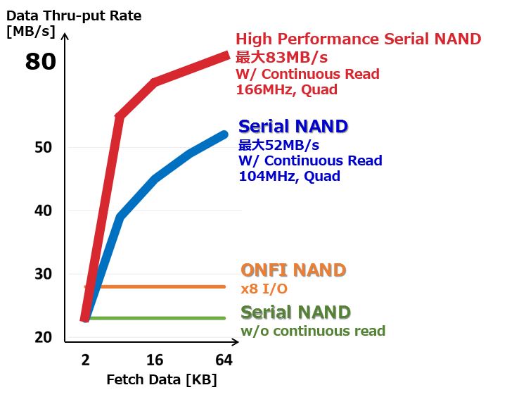
Fig. 1: in the past, SPI NOR has offered faster Read speeds than serial NAND. (Image credit: Winbond)
Latency is a key performance parameter in AI systems. An inference engine implementing a machine learning algorithm locally must perform hugely complex computing operations often in a matter of milliseconds. This calls for fast data Read performance.
The first generation of 104MHz QspiNAND Flash from Winbond achieved a maximum read throughput rate of 50MB/s in Continuous Read mode. For comparison, 133MHz Quad SpiNOR Flash offers maximum read throughput of 80MB/s (see Figure 1).
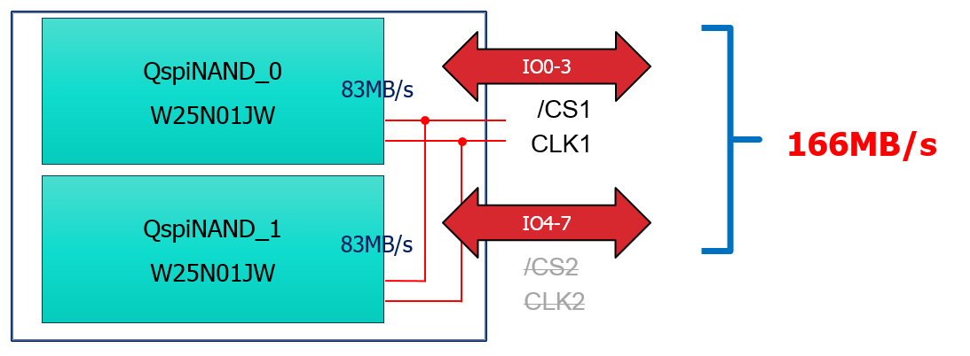
Now Winbond has introduced the second-generation W25Nxx JW QspiNAND series of devices which supports a higher clock speed in STR (single transfer rate) mode of 166MHz (83MHz in double transfer rate mode), for a maximum read throughput of 83MB/s. This read throughput rate can be doubled to 166MB/s through use of the W72N series of dual QspiNAND Flash products, which are made of two dies in a single package to provide 8 I/Os in a dual x4 configuration.
Innovative control software enables the host controller to operate a W72N via a single Chip Select command (see Figure 2).

Fig. 2: Winbond’s dual QspiNAND offers a maximum Read speed of 166MB/s. (Image credit: Winbond)
This fast Read performance results in low latency in AI systems. The high performance of Winbond QspiNAND Flash also supports fast OTA update operations, to minimize downtime. Program mode throughput of the new 1Gbit W25N01JW QspiNAND product is 8.5MB/s, compared to 0.36MB/s for the 256Mbit W25H256JV, a Winbond SpiNOR Flash product. Erase time for a 128Kbit block is 2ms for the QspiNAND product, compared to 150ms for a 64Kbit block in the SpiNOR product.
Total programming time for 1Gbit of data is nearly six minutes – 356 seconds – for the SpiNOR device versus just 15 seconds for the second-generation QspiNAND product.
Easy to Integrate in Embedded Systems
The move to integrate AI functions into embedded systems, then, gives OEMs a strong reason to evaluate serial NAND Flash as a replacement for more costly SPI NOR at densities of 1Gbit and higher. The implementation of serial NAND in Winbond’s second-generation QspiNAND products eases this transition, not only in the provision of simple 1-bit ECC, but also in the operation of the QspiNAND interface itself: it is software-compatible with the familiar SPI NOR interface, and only requires the implementation of five new commands to control ECC and Look-Up Table (LUT) functions which are specific to NAND Flash technology.
In addition, QspiNAND devices such as the 1Gbit W25N01JW are supplied in industry-standard footprints and pin-outs, so they may be used as drop-in replacements for SPI NOR Flash parts in existing designs.
And integration of this advanced, reliable serial NAND technology into embedded systems is further facilitated by the ecosystem of SoC providers which supports it, including NXP Semiconductors, STMicroelectronics and Renesas. NXP, for instance, has built a Winbond SpiStack NOR+NAND co-packaged device into its FRWY-LS1012A development board for the LS1012A edge computing processor. In this implementation, a Winbond QspiNAND device stores the board’s Linux® operating system code, while a small Winbond SpiNOR die stores the chip’s boot code.
Available today in 1Gbit density, second-generation QspiNAND Flash technology is scalable to densities of 2Gbits, 4Gbits and more. It therefore provides the roadmap that embedded developers need to guarantee reliable storage of the growing code bases through which they will implement ever more sophisticated AI technology at the edge.
By Syed S. Hussain, Director Segment Marketing, Winbond Electronics Corporation America


 English


