NOR Flash has been a dependable technology in vehicles for many years, and today is used in various automotive systems, including the instrument cluster and in infotainment and telematics systems (see Figure 1). In these applications, this non-volatile memory provides storage capacity for application code, offering the advantages of reliable operation and Read speed fast enough to support Execute-in-Place (XiP), in which a host processor runs code directly from Flash, bypassing external DRAM.
NOR Flash is also playing an important role in emerging implementations of the ADAS (Advanced Driver Assistance Systems) concept, which in cars available today is already performing semi-autonomous highway-driving functions such as adaptive cruise control and lane-keeping. The pace of development in autonomous driving technology is extremely fast, and so in the next few years more and more of a vehicle’s activity will be controlled by electronics systems containing Flash.
In ADAS, as well as in the instrument cluster and elsewhere, Flash is a component in systems which are safety-critical: any uncontrolled failure of such a system would have the potential to render the vehicle unsafe or uncontrollable. To manage and minimise the risk of systems failing to operate as specified, the automotive industry has implemented the ISO 26262 Functional Safety standard, which:
- imposes a requirement at the design stage to perform rigorous analysis of the ways in which a system’s designed functions can fail
- specifies very low maximum failure rates for complete systems
- requires systems to have the ability to detect functional failures reliably and quickly
- requires systems to put in place robust means to survive safely, and recover from, any foreseeable functional failure
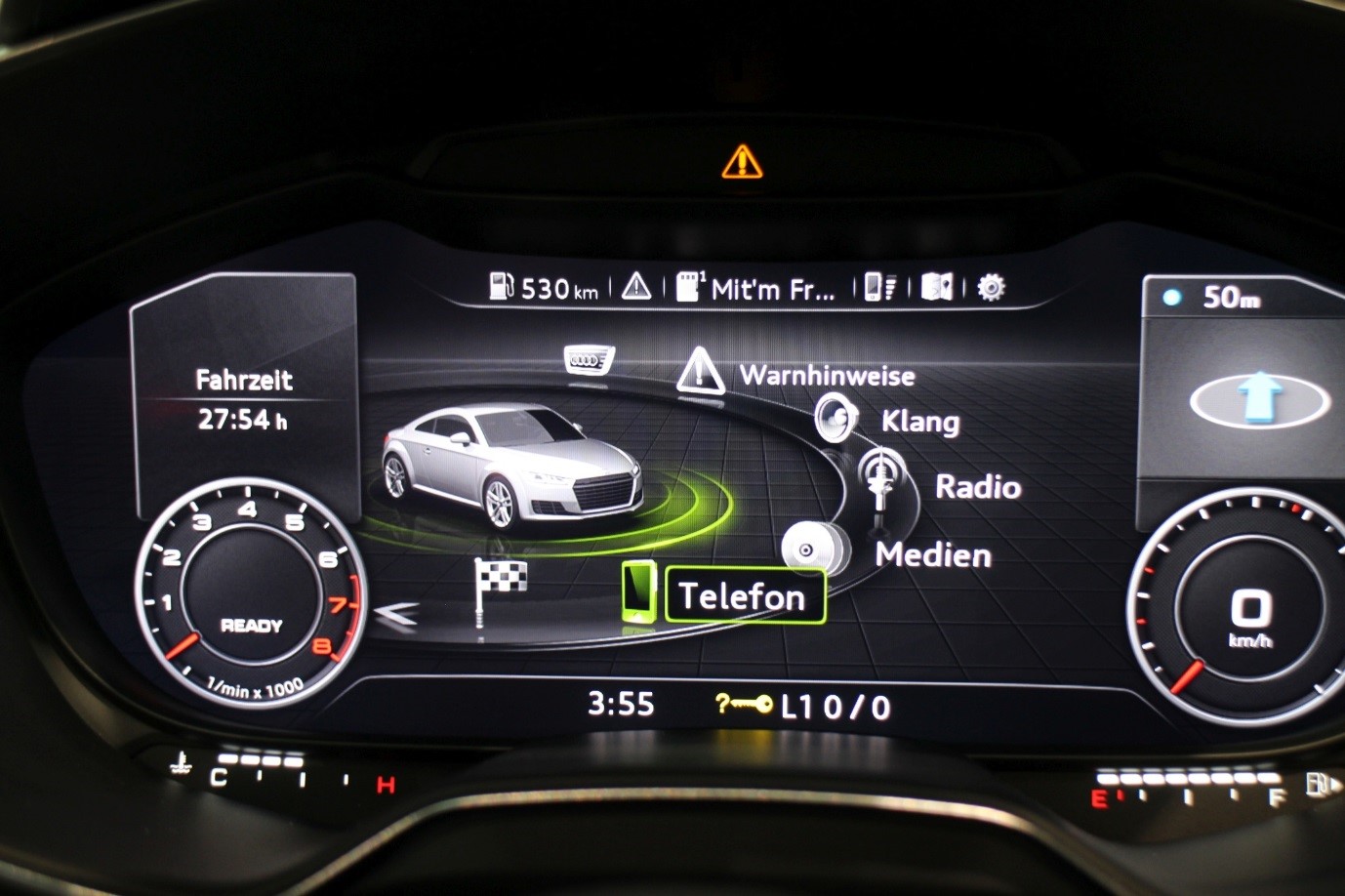
Fig. 1: the virtual instrument cluster in a 2014 Audi TT. NOR Flash is widely used to enable instant display of essential cluster information at start-up. (Image credit: Robert Basic under Creative Commons licence.)
Automotive systems OEMs are therefore starting to demand a new breed of Flash ICs which can support the requirements of functional safety design at the system level better than previous generations of devices. This article studies the mode of operation of conventional NOR Flash ICs, and explains the features that new automotive serial Flash products will need to offer if they are to fully support system designers’ efforts to comply with the ISO 26262 standard.
These functional safety features will likely be seen both in serial NOR Flash – the Flash memory type most often used today in embedded systems for boot code storage – and in Single Level Cell (SLC) NAND Flash. QspiNAND is in fact a valid alternative to NOR Flash for code storage in applications that do not require a high number of Program/Erase cycles, and that do not need to implement XiP. Winbond’s SLC NAND technology is built in a 46nm process, which offers proven high quality and is preferable in functional safety applications to QspiNAND products fabricated at new, smaller geometries. It also offers data retention periods comparable to those of 55-65nm NOR Flash.
The advantage of QspiNAND is its inherently lower cost – a NAND Flash bit cell is four times smaller than that of a NOR Flash cell. Supplied by Winbond with an on-board Error Correcting Code (ECC) engine and supporting high-speed continuous/sequential Read capability across page and block boundaries, QspiNAND is now being seriously considered by designers of automotive functional safety applications alongside the NOR Flash which is the subject of this article.
Exposing Diagnostic Data to View in NOR Flash ICs
It’s important to state that NOR Flash memory technology is very reliable, and devices’ operating lifetime is highly predictable. NOR Flash ICs have proved their qualities in the field, and automotive OEMs’ preference for the technology is based on experience of its use in millions of vehicles on the road today. For perspective, the ISO 26262 standard specifies reliability and other parameters in four ‘ASIL’ grades (Automotive Safety Integrity Level). The most stringent grade, ASIL-D for the most safety-critical systems such as steering or brakes, sets a maximum system-level failure rate of <10 FIT (Failure In Time) – a measure of the failure rate per billion device-hours (see Figure 2). At the level of individual components such as a NOR Flash IC, this calls for a maximum failure rate of far below 10 FIT.
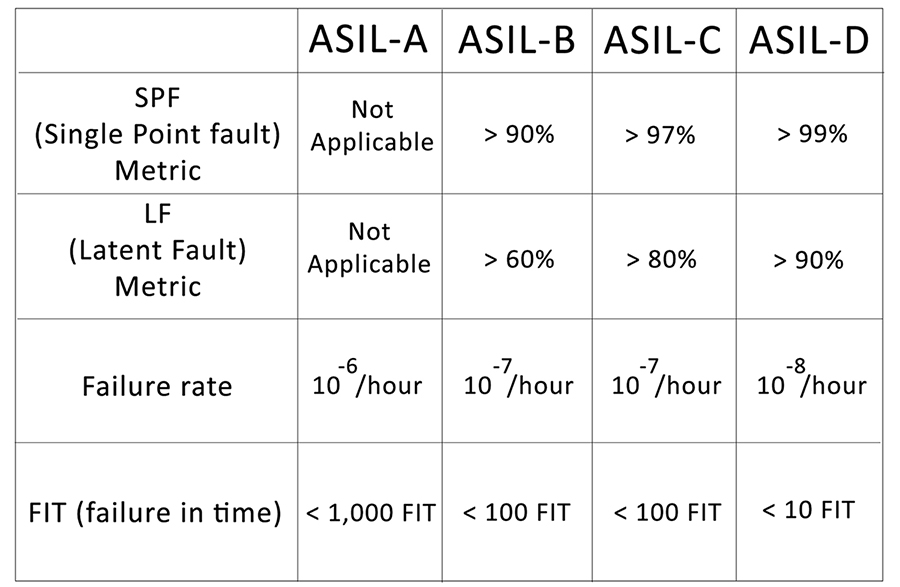
Fig. 2: minimum detection rates for single-point and latent faults, and maximum failure rates as specified by the ISO 26262 standard
Nevertheless, automotive manufacturers’ ISO 26262 compliance efforts call for a way to identify any fault that could theoretically still occur in a NOR Flash IC. And at the time of writing (May 2017), NOR Flash ICs are supplied to automotive OEMs as a memory ‘black box’. Functions which maintain data integrity and data retention are, in conventional devices, inaccessible to the user. This closed operation is in conflict with the principles of functional safety, which require the host system to monitor component parts for faults, or for irregular behaviour that indicates a fault is likely to occur, and to implement counter-measures aimed at maintaining proper functioning.
This means that NOR Flash ICs intended for use in ISO 26262-compliant systems must make diagnostic data available to the host controller, and provide ways in which the host can modify the IC’s operation in response to a heightened risk of failure indicated by the data.
Two main features of a NOR Flash IC provide these data:
- the ECC engine, which maintains data integrity by detecting and correcting bit errors in Read operations
- a User Mode which enables periodic testing of the ECC engine’s operation
How ECC Data Supports Functional Safety Operations
In conventional NOR Flash ICs, the ECC engine operates in the background, detecting and correcting bit errors with multi-byte granularity silently, without alerting the host controller.
In fact, however, these ECC data may be used to facilitate functional safety compliance in various ways. An ECC engine is capable of correcting single-bit errors (when there is only a single bit variance between the main data bit and the parity bits); and of detecting (but not correcting) double-bit errors.
By providing a status register to the host controller, a NOR Flash device can indicate whether the most recent Read operation had one of three possible outcomes:
- good data with no error correction required
- good data after error correction
- bad data that were not able to be corrected
This ‘after the fact’ information can be used to help maintain long-term data integrity, as we shall see. But ISO 26262 requires automotive systems to detect faults when they occur, and to deploy counter-measures immediately. In new automotive NOR Flash ICs from Winbond, real-time error information may be provided via a dedicated Error pin. This pin may be asserted to indicate the exact location of uncorrectable data. There is also an option for the user to select whether the Error pin will indicate corrected single-bit errors, or detected and uncorrectable double-bit errors.
The host may then use the information from the status register, from the Error pin, or from both, to build an error register – effectively a ‘map’ of the NOR Flash array, logging the locations of bit errors. The host may then set a threshold, so that when the number of errors occurring at any one location, such as a particular block, exceeds the threshold, that location is ‘retired’ from the memory. This is a sensible precautionary measure: the repeated occurrence of corrected single-bit errors in a particular block of memory cells might indicate that the block is weak, and at risk of premature failure.
Measures to Identify a Latent Failure in Automotive Systems
So far, the measures described are concerned with the handling of single-point faults, for which the ISO 26262 standard specifies minimum detection rates for each ASIL grade. But the standard also requires automotive systems to detect ‘latent faults’. A latent fault is a fault which does not violate functional safety requirements on its own, but which can violate them in conjunction with a second fault.
In a NOR Flash IC, there is potential for such a latent fault – a malfunctioning ECC engine is an example. In normal operation, NOR Flash technology is highly reliable and rarely requires error correction. So as long as an ECC engine failure does not cause it to wrongly correct good bits, the failure would normally go unnoticed. But when a single bad bit goes uncorrected because of the failed ECC engine (a latent fault), the two faults in combination pose a risk to functional safety.
To enable detection of a latent ECC engine fault, Winbond’s automotive NOR Flash ICs provide special User Mode and ECC Encoder Read commands: this enables the user to inject a main data pattern into the memory, and to read back from the ECC engine the main data and the parity data that it generates. If the parity data are incorrect, the ECC engine can be flagged as faulty.
Likewise, the User Mode may be used to check ECC decode operation: in User Mode, the user loads main data and parity data into the ECC engine, and with a special ECC Decoder Read command the main data may be read back. Single-bit and double-bit errors may be introduced into the main data and parity data to check whether the ECC engine performs single-bit error correction and double-bit error detection properly. Winbond’s recommendation is that this ECC engine check should be performed every time the system powers up.
New Functional Safety Features Available in Automotive NOR Flash
In response to demand from manufacturers of ADAS products and other automotive systems, Winbond is now integrating the functional safety features described above into a new family of automotive NOR Flash products. The Quad 3V family, featuring a maximum 80MB/s data transfer rate, is available for sampling in a density of 256Mbits as of May 2017. A 512Mbit part (two stacked 256Mbit dies) will be available in the second half of 2017. In 2018, Winbond will release a 512Mbit part with a monolithic die, and a 1Gbit part made from two 512Mbit stacked dies.
Winbond’s Octal 1.8V family, featuring a data rate of more than 300MB/s, will be available in densities from 256Mbits, with samples planned for late 2018. Proliferation into other densities will follow later.
Winbond also offers QspiNAND products with functional safety features: as of May 2017, products are available for sampling at densities of 512Mbits, 1Gbit and 2Gbits (made of two stacked 1Gbit dies).
Winbond QspiNAND products, such as the 1Gbit W25N01GV, support functional safety compliance by providing information to a status register showing whether data read out were good without ECC, good with ECC, or uncorrectable. The QspiNAND page size is 2kbytes and 1-bit embedded ECC is offered at the sector level (512 bytes). This means that up to 4-bit correction can be performed on a 2kbyte page. Winbond QspiNAND also offers the ability to read the location of a failed page when prompted by an additional user command.
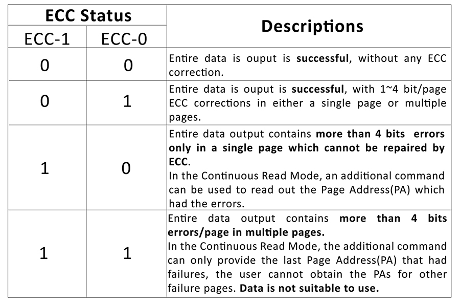
Fig. 3: the error log in Winbond QspiNAND helps identify potential weak cells or blocks
By providing both SPI NOR and QspiNAND solutions for functional safety applications, Winbond offers the user the freedom to select the appropriate Flash memory type for the requirements of their design.
For more product information, please visit Winbond Code Storage Flash Memory
By Anil Gupta, Technical Executive, Winbond Electronics Corporation America
Anil Gupta has 35 year experience in Non-volatile memories. He is Technical Executive at Winbond Electronics and currently managing Technical Marketing for Flash products in Europe and Israel. He presented 2 papers at Electronica, Nov 2018 in Munich to explain major advantage offered by Serial NAND in OTA update applications for autonomous driving, and have presented multiple papers in Flash Memory Summits. He developed and led Industry’s first commercially successful SPI NOR product line at Atmel during 1995~2007. He designed and presented key paper in 1982 IEEE (ISSCC) conference on Industry’s first EEPROM to eliminate external high voltage with on-chip charge-pump while at SEEQ.


 English

