The edge artificial intelligence (AI) chipset market is expected to exceed the cloud AI chipset market for the first time in 2025. According to global tech market advisory firm, ABI Research, the edge AI chipset market will reach US$12.2 billion in revenues, outpacing the cloud AI chipset market, which will reach US$11.9 billion in 2025. Edge AI includes smart phones, wearable devices, smart vehicles, and smart home/industry/city. Above of them, smart home will play a key driver role of edge AI market.
Most AI training workloads happen in the public and private clouds. Traditionally, the centralization of these workloads in the cloud brings the benefits of flexibility and scalability. However, driven by the need for privacy, cybersecurity, and low latency, performing AI inference workloads is preferred on gateways, devices, and sensors. Recent advancements in key domains, including new AI learning architecture and high-performance computational chipsets, have played a critical role in this shift.
Edge AI computes the data as close as possible to the physical system. The advantage is that the processing of data does not require a connected network. The computation of data happens near the edge of a network, where the data is being developed, instead of in a centralized data-processing center. One of the biggest benefits of edge AI is the ability to secure real-time results for time-sensitive needs. In many scenarios, sensor data can be collected, analyzed and communicated straightaway, without having to send the data to a time-sensitive cloud center.
In addition to applying in smart phones, deep learning is also used in IoT devices (also known as AIoT). Edge AI bring a new concept for legacy IoTs. Nevertheless, the computing power of MCU, which is a traditional processing unit in IoTs, is too weak to doing deep learning. At this moment, there are two kind of hardwired mechanism to help MCU: DSP or the dedicated accelerator (called as Deep Neural Network/DNN). These hardwired mechanism could be implemented as IP or a chip.
The fundamental component of both the convolution and fully-connected layers, which are main algorithms of DNN, are the multiply-and-accumulate (MAC) operations. In order to achieve high performance, highly-parallel computing methods are frequently used. Many iterations of weight which are commonly stored in DRAM are updated according to different training styles.
Regardless of above mechanism, DRAM throughput is key to DNN. Therefore, choosing a proper DRAM is critical to AIoT application. Unlike cloud environment, low power is a concern in edge computing. The planner of AIoT device must seek to balance performance and low power. Apart from power and performance, the density of DRAM integrated in AIoTs devices usually only need low density (1~2Gb) rather than commodity one (8~16Gb per die).
Winbond Electronic Corp.’s 1Gb LPDDR3 DRAM die was one such example with AI company Kneron having selected it for its latest system-on-chip (SoC), the KL720. It’s one of several SOCs the company offers that being used in a variety of edge devices, including battery-powered applications such as smart locks and drones that take advantage of a 512Mb LPDDR2 from Winbond.
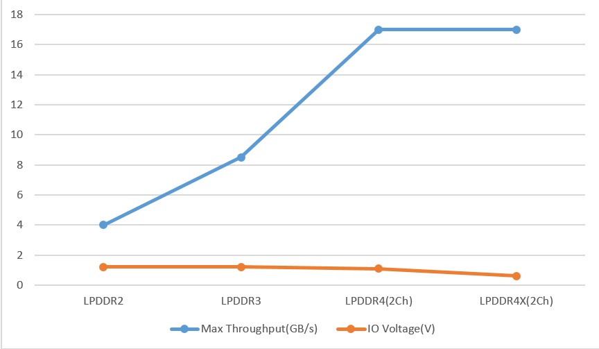
LPDDR3, delivering a maximum bandwidth 8.5GB/s with a dual 1.2V/1.8V supply, enable customer devices like Kneron’s KL720 to process 4K, Full HD or 3D sensor video images in real time to support AI applications such as face recognition in security cameras or gesture control in public kiosks, as well as perform natural language processing.
Beyond the needs of Kneron and the applications for its KL720 SoC, there are potential uses for devices with the density and bandwidth of Winbond’s LPDDR3 DRAM in automotive applications such as Advanced Driver Assistance Systems (ADAS), which employ cameras that must process video images in real time. Meanwhile, there are many opportunities for IoT endpoints that need to do basic AI inference, which require low densities, but high bandwidth.
LPDDR4/4x x32 has an almost double throughput than LPDDR3, same advantages as what LPDDR3 has with LPDDR2, shown in Fig.1. In power consumption, the IO voltage of LPDDR4x is 0.6(V), in contrast that LPDDR4 is 1.1(V). Although JEDEC has already published the latest LPDDR5 standard, the density of LPDDR5 just released into the market is still too high to be applied in the AIoTs. At this moment, LPDDR4x is still the best choice, if we need more AI computing power than what LPDDR3 could provide.

Fig.1
Winbond owns self-built wafer fabs, and is one of the top four IC makers that can simultaneously provide DRAM and NOR/NAND Flash. The capacity of Winbond LPDDR4/4x DRAM series is 1~4Gb with 25nm technology node which is self-developed by Winbond, and the speed could be up to 4266Mbps. In addition to the supply type of known good die, Winbond also provides the standard 200BGA package.