The two broad categories of non-volatile Flash memory are known by every hands-on system designer.
There is NOR Flash, which is a robust and reliable memory which can store data for long periods. It is produced in relatively low densities of 256Mb and less, and has a relatively high cost-per-bit.
And there is NAND Flash, a memory technology which is prone to bit errors, but which offers the advantages of high density – as of February 2018, advanced 3D NAND parts were available in densities as high as 6Tb – and very low cost-per-bit.
This gives designers a simple, ready-made rule of thumb to guide their selection of Flash memory type for any given application:
- for code storage, specify NOR Flash to provide reliable performance and long data retention. It is suitable for intensive program/erase cycling.
- for data storage, specify NAND Flash for its ability to provide very high capacity at very low cost, as long as the use case can tolerate a high bit error rate.
This summarises the industry’s general assumption about the uses of NOR and NAND. And like most widely-held views, it’s true – but only partly so. In fact, the technologies of both NOR and NAND Flash memory are changing at different rates, and this affects their comparative benefits and drawbacks.
There are certain circumstances today in which a certain type of NAND Flash IC may be preferable to a NOR Flash device for storage of mission-critical code. Such NAND chips can offer performance as reliable and robust as NOR Flash ICs, with similar endurance, but at less than half the cost-per-bit.
This article describes these circumstances, and the reasons why NOR Flash cannot be assumed to be the right technology type for code storage in all cases.
Why The Choice of Flash Technology Matters Today
For many embedded applications, the possibility that serial NAND Flash with an SPI interface could replace SPI NOR Flash for code storage is of little or no relevance. In embedded designs with a code base of up to 256Mb, a NAND Flash memory solution would be no cheaper than the equivalent NOR Flash circuit: at low densities of 256Mb and below, peripheral functions such as logic and a charge pump are big components of the cost of the chip, and the memory array alone is not a dominant component. The lower the memory density, the more this is the case. Here, the smaller size of a NAND memory cell compared to a NOR memory cell is of negligible benefit. At densities of 512Mb and above, most of the die area is occupied by the memory array, so the lower cost-per-bit of a NAND Flash cell gives it a marked advantage over NOR Flash.
A memory capacity of 256Mb is not sufficient, however, for an emerging category of embedded applications; this is most clearly seen in vehicle systems in development today. Sophisticated automotive applications from Advanced Driver Assistance Systems (ADAS) up to fully autonomous driving systems will create much larger code bases. Today, automotive systems OEMs are specifying memory systems for code storage with a capacity of as much as 2Gb (or 256MB).
So designers of automotive systems, who operate in an acutely cost-conscious environment, will want either the cost of NOR Flash at higher densities to drop, or for lower-cost NAND to be made suitable for code storage.
And here designers’ wishes come up against the hard reality of NOR Flash technology’s rate of development.
The End of NOR Process Scaling
Process shrinkage is the semiconductor industry’s time-tested method of delivering ever greater functionality at ever lower cost. For many years, this was as true of NOR Flash ICs as of any other type of semiconductor. In 1986, the leading edge of NOR Flash fabrication technology was at the 1.5µm node. Around two decades later, NOR Flash devices were being fabricated at the 65nm node.
Process technology for NAND Flash has continued to shrink in the years since: today, the highest density 3D NAND Flash ICs used in smartphones and computing equipment may be fabricated at a 1xnm node.
NOR Flash scaling, however, has ground to a halt. Implementing the 65nm node had already proved to be much more difficult than any previous node. Then in 2008, Intel published a paper describing a new 45nm Flash fabrication process. As of March 2018, however, some ten years later, only one or two manufacturers supply 45nm NOR Flash products. Other suppliers have a roadmap for 4xnm NOR Flash, but their technology is still in development.
The industry has discovered that the dimensions of certain elements of a NOR Flash circuit push manufacturing capabilities to their limit. If 65nm was a speed bump for NOR scaling, 45nm appears to be a complete barrier, and there is today no prospect of scaling NOR Flash beyond this node.
This means that, for automotive systems manufacturers, there will be no Moore’s Law-induced drop in NOR Flash cost-per-bit, and process scaling will not blunt the effect on bill-of-materials cost due to the increasing requirement for code storage resulting from the introduction of advanced applications such as autonomous driving.
So can NAND Flash instead, with its much lower cost-per-bit, step in to replace NOR Flash for code storage in these safety-critical applications?
To answer this question, we need to understand the mechanism by which data may be lost from a NAND Flash IC.
Common Failure Modes of NAND Flash Memory
There are two main ways in which bit error may occur in the normal course of a Flash IC’s operation:
- bit errors may occur in writing to the memory array
- electron leakage from Flash memory cells can result in loss of data after a period of time, creating potential read errors. Operation at extreme high temperature has the effect of accelerating electron leakage and thus shortening the average length of data retention across a Flash device.
The risk of data loss caused by Read bit error can be eliminated by the implementation of robust Error Correcting Code (ECC). All Winbond serial NAND Flash devices on 46nm technology are shipped with on-board 1-bit ECC.
Electron leakage, on the other hand, cannot be prevented. But what is the risk that it poses? This is simply a matter of calculating the initial number of electrons in a cell after it is programmed, and the rate of leakage. Put simply, if a cell starts with many electrons and loses them at a slow rate, it will take a very long time before the charge in the cell has dropped so far that it cannot be reliably read.
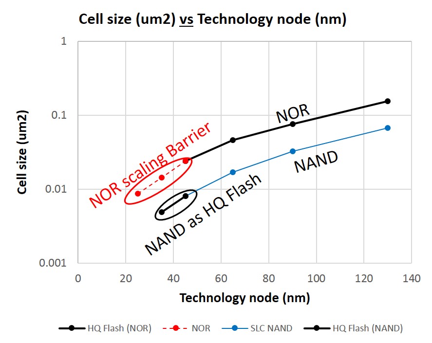
Initial electron count is a function of cell size. As Figure 1 shows, for any given process node, a serial NAND cell is smaller than an SPI NOR cell. This is an inherent feature of the two technologies, and explains why NAND offers a lower cost-per-bit. (A smaller die is a cheaper die.)

Fig. 1: comparison of NOR and NAND cell sizes with extrapolation of NOR cell size if NOR technology scaled down to 2xnm. If a 2xnm NOR device could be produced, its cell size would be similar to that of today’s 4xnm serial NAND devices. (Image credit: Winbond) (Appendix: reference 1)
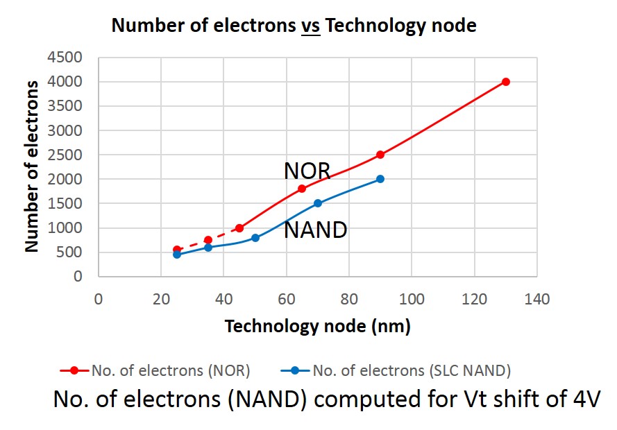
A comparison of the electron counts of SPI NOR and of Single-Level Cell (SLC) serial NAND Flash devices is shown in Figure 2. This helps explain the emergence of NOR Flash as the ‘reliable’ memory type. A NOR Flash IC fabricated at the 130nm node would contain 4,000 electrons per cell. Conservatively assuming a leakage rate of 1 electron per month, or 120 electrons over 10 years, the effect of leakage on the charge level in the cell is negligible.
Electron leakage, though, becomes a more acute problem the smaller the process geometry becomes: smaller cells hold less charge. This is as true of NOR Flash as it is of NAND Flash circuits.
The minuscule circuit features of today’s 1xnm MLC or Three-Level Cell (TLC) NAND Flash ICs can result in specified data retention times as short as a few hours or days in some operating conditions. These leading-edge devices require complex scan-and-refresh mechanisms to periodically recharge the cells.
Mission-critical automotive applications, however, have zero tolerance for data loss over a long product lifespan of at least ten years. And automotive designers do not want to deal with the complication and risk of implementing scan-and-refresh functions.
 Fig. 2: even down to the 3xnm node, a NAND Flash cell will contain above 500 electrons – the required number for classification as a ‘High Quality’ memory. (Image credit: Winbond) (Appendix: reference 2)
So what is the minimum electron count required for a device to qualify as a ‘High Quality’ memory for use in high-reliability applications? The scientific literature and judgment suggests that 500 electrons per cell can be considered a quality threshold, as such a cell would still retain 75% of stored electrons after 10 years assuming one electron is lost per month. Figure 2 shows that serial NAND at 46nm and at 3xnm exceeds this value.
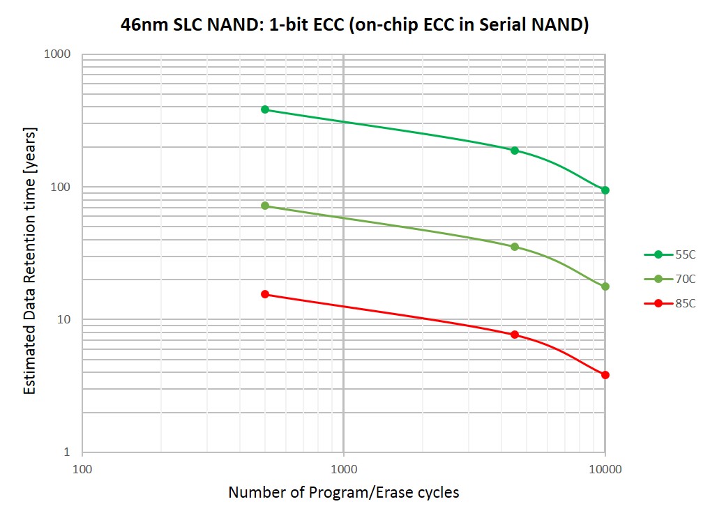
This threshold for Flash memory quality is borne out by the performance of a new class of High Quality (HQ) SLC serial NAND Flash devices developed by Winbond, and fabricated in Winbond’s 46nm process. These parts are subject to special screening and testing procedures. Data retention performance at various operating temperatures is shown in Figure 3.

Fig. 3: data retention performance of Winbond HQ serial NAND ICs. (image credit: Winbond)
Figure 3 shows that data retention time of Winbond’s HQ serial NAND devices is comparable to that of today’s NOR Flash devices fabricated at 65nm and below.
More relevantly to advanced automotive code-storage applications, data retention in an HQ serial NAND device subject to a maximum of 100 Program/Erase (P/E) cycles, and operating at a high temperature of 85°C, is 25 years. In an automotive application, code is highly unlikely to be subject to as many as 100 P/E cycles. Winbond test data also show that the devices support more than 15 years’ data retention at 70°C after 10,000 P/E cycles, which is comparable to the performance of NOR Flash products on the market today.
The Winbond HQ serial NAND Flash devices benefit from the same cost advantage over NOR Flash as any other type of NAND, such as ONFi NAND Flash. The cost-per-bit of an HQ serial NAND Flash IC from Winbond is typically less than half that of the equivalent SPI NOR Flash solution at densities of 512Mb and above.
Easy Implementation in Automotive Circuits
Other features of the Winbond HQ serial NAND parts make them as easy to integrate in automotive circuits as NOR Flash parts are. When shipped, and for up to 100 P/E cycles, they are guaranteed to contain no bad blocks. This means that, in code storage applications, there is no need to implement bad block management (BBM) in an SoC or microcontroller. BBM would normally be required when using a conventional serial NAND part.
The Winbond devices also support boot directly from serial NAND Flash thanks to additional features such as automatic loading of page-0 at power-up, on-chip ECC and NOR Flash-compatible Read commands. Winbond’s HQ serial NAND Flash devices are intended for use in code-shadowing applications that include a DRAM supporting the SoC or host processor.
For designs migrating from SPI NOR parts at densities of 256Mb (32MB) and below to the serial NAND parts in 512Mb or 1Gb densities, the pin-out and footprint remain the same, providing for a smooth transition from SPI NOR to serial NAND.
HQ SLC NAND Flash: Large Cost Benefit, No Performance Penalty
The barrier to NOR Flash scaling beyond the 45nm node means that automotive system manufacturers will face a huge bill-of-materials cost penalty if they decide to meet the requirement for increased code storage capacity in new applications with expensive SPI NOR Flash devices.
At a cost-per-bit typically less than half that of SPI NOR Flash in 512Mb, 1Gb and 2Gb densities, Winbond’s HQ serial NAND Flash parts provide automotive manufacturers with a new way to provide sufficient code storage capacity at a much lower cost while meeting the very high standards of reliability and robustness specified in safety-critical automotive systems.
Appendix: image references
- Cell area graph: NOR Flash cell sizes drawn from ‘A 45nm NOR Flash Technology with Self-Aligned Contacts and 0.024µm2 Cell Size for Multi-Level Applications’, Fastow et al., Intel Corporation, IEEE 2008; and ‘ETOX™ Flash Memory Technology: Scaling and Integration Challenges’, Fazio et al., Intel Corporation, Intel Technology Journal, 2002. NAND Flash cell sizes calculated as 2F x 2F.
- Electron count graph: NOR Flash electron counts drawn from ‘Future Directions and Challenges for EToxFlash Memory Scaling’, Greg Atwood, Intel Corporation, IEEE Transactions On Device and Materials Reliability, 2004, and ‘Advanced Flash Technology Status, Scaling Trends & Implications to Enterprise SSD Technology Enablement’, Yoon and Tressler, IBM Corporation, Flash Memory Summit, 2012. NAND Flash electron counts computed for Vt shift of 4V.
By Anil Gupta, Technical Executive, Winbond Electronics Corporation America
Anil Gupta has 35 year experience in Non-volatile memories. He is Technical Executive at Winbond Electronics and currently managing Technical Marketing for Flash products in Europe and Israel. He presented 2 papers at Electronica, Nov 2018 in Munich to explain major advantage offered by Serial NAND in OTA update applications for autonomous driving, and have presented multiple papers in Flash Memory Summits. He developed and led Industry’s first commercially successful SPI NOR product line at Atmel during 1995~2007. He designed and presented key paper in 1982 IEEE (ISSCC) conference on Industry’s first EEPROM to eliminate external high voltage with on-chip charge-pump while at SEEQ.