With more complex application being put into modern electronic devices, higher throughput is expected within the IC. We could achieve this goal by speeding up the clock, or by adding more IOs. A higher clock will lead to Signal Integrity (SI) issue, like crosstalk, Electromagnetic Interference (EMI). This phenomenon will be exponentially worse with continuing escalating clock speed. On the other hand, adding IOs could transmit or receive more data at the same time without handling the above issues.

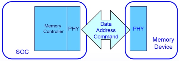
Fig. 1: Today’s DRAM peripheral environment
Widening data path could be alternative way to rising throughput. Therefore, we could see more connection between ICs, including SOC and DRAM (Fig. 1). The connection needs to be tested in order to be confirmed successfully. The test cost which includes time and tool expense will increase with the number of IC Pads. In addition, System in Package (SIP) is more popular in modern electronic devices. For instance, iPhone X uses more SIPs than the first generation of iPhone does. The testing expense of the connection will be higher once more SIP solution is being used in the consumer devices
Why is it difficult in coping with SIP connection? SIP categories could be divided two categories: Wire bonding or flip chip. However, regardless of the way in which it is used in SIP, the connection is necessary to check inside the package, not in PCB which was commonly used a decade ago. Device makers will suffer a significant loss if they cannot find a connection failure after SIP is finished.
Traditionally IC design vendors suffer the similar IC test problems. In today’s IC test strategy, Design for Testability (DFT) and Built In Self Test (BIST) are commonly used. D-type Flip-Flop in the whole chip will be changed to series cascade to receive an input long sequence and to check correctness at the output pin (Fig. 2).

Fig. 2: Boundary Scan is traditionally used to Built-In-Self-Test in internal IC
The JEDEC industry standard for DRAM, GDDR3, devices do specify an automatic checking way, Boundary Scan mechanism, which can be applied when transferring predetermination of data to valid whether the connection is correct or not. GDDR is often considered to be used in a video game environment. Through its high bandwidth and low latency property, Graphic Processing Unit (GPU) could access rendering context peripheral GDDR chips fast in the graphic card. Instead of detecting IC internal manufacture fault with traditional boundary scan technology, GDDR’s mechanism could detect PCB level connection failure in the graphic card.
Winbond provides similarly to this standard, which could give customers more confidence and will make it easier to get used to this method. SIP is often used in mobile application due to its tight space budget. SIP makes detecting connection faults even more difficult. If IC could have a self-testing way to detect connection failure inside the package, it will save a lot of effort including the test and cost penalty before the product goes into the market. Self-test mechanisms also have another advantage in diagnosing itself after shipping to end customers, which will reduce it by a significant amount of time during the Failure Analysis procedure.
New Winbond Boundary Scan mode
Winbond device is built with a boundary scan chain for users to test the connectivity between the memory controller and the memory device itself. The boundary scan chain provides a simply way to check the status of connection between the memory controller and the memory device. The boundary scan chain is able to be enabled by a SEN input. All the connection status of each IO between the memory controller and memory device will be latched onto by the scan chain in parallel and be read out from a dedicated output pin serially.
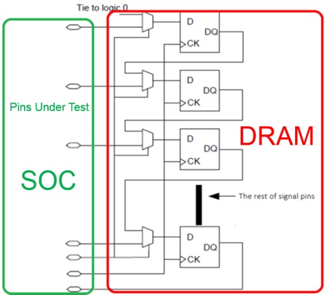
SOC side could send parallel predefined patterns of Pin Under Test (PUT) to DRAM side when DRAM is operated in this mode (Fig. 3). By being pushed with each SCK(scan clock) pin, SOC can finally check correctness at SOUT(scan out) pin within a series sequence. This method could be used in a discrete chip or in the SIP scenario.

Fig. 3: The connection check could be done with Boundary Scan
Operational control
There are two modes of boundary scan operations:
- The first mode is the Stand-Alone mode. In the Stand-Alone mode the device is supposed to support the Boundary Scan functionality only, the user does not intend to operate the DRAM in its ordinary functionality after or prior to the entering of the Boundary Scan functionality. The purpose of the Stand-Alone mode could be a connectivity test at the manufacturing site.
- The second mode is the regular device functionality. With this common mode the boundary scan functionality can be enabled after the device has been initialized by the regular power-up and device Initialization sequence. When the boundary scan functionality is left, the regular device initialization sequence has to be re-iterated.
Roadmap for roll-out of Boundary Scan
The Winbond roadmap sees the Boundary Scan function being introduced into a number of LPDDR devices over the coming months, alongside the 2Gbit W97BH2M series which is already in the sample stage. New devices with Boundary Scan capability will include 4Gbit LPDDR4 parts in the first half of 2019.
These new parts offering the Boundary Scan option will give manufacturers of mobile phones and other devices a new means to reduce total cost attributable to the DRAM and to take advantage of additional time savings with an easy way in being operated in Boundary Scan mode.
By Hsiu Min Lin
Mobile DRAM Marketing Manager, Winbond


 English


