Booming of Massive IoT
According to the mobility report published by Ericsson in June, 2020, Massive IoT, including NB-IoT and Cat-M, continues to be deployed around the globe. Owing to the fact COVID-19 blocks transportation, the process of penetration is lower than we expected. Most of IoT applications are still connected through 2G or 3G technology. In 2019, the estimated number of massive IoT applications have grown to triple and will reach approximately 100 million by the end of 2020.
As Ericsson estimates by the end of 2025, NB-IoT and Cat-M will account for 52% of all cellular IoT devices. Asia region will be fastest growth market and volume of device in this region will increase to 67% of all shipment before 2026.
As for 3GPP standard progress, Release 15 has enhanced the stability and application field regardless of NB-IoT or Cat-M. Release 16 which is just frozen in July 3, 2020 will strengthen further on network efficiency and deploy current NB-IoT to be operated in 5G environment. In the future, Release 17 will extend specification of bandwidth aggregation and of lower latency, continuing to develop and exploring potential application in order to stimulate cellular IoT penetration based on 5G NR foundation.
Semiconductor vendors' action for IoT
For IoT applications, various design considerations such as low cost, low power consumption, and computing efficiency must be met in order to gain widespread adoption in the market. Especially, for battery-powered devices such as smart speakers and smart meters, battery life has become the key to the success of the product, in addition to the rich IoT function and easy-to-use human interface. This makes low power consumption increasingly important. To achieve long battery life, in addition to using power consumption MCU, the other low-power peripheral components should also be considered.
Many mobile devices have the similar architecture in Fig.1. Such a block diagram exists in tablet or smart watch. Wi-Fi/BT and cellular module are in charge of communication. Sensors (like the touch panel) are dedicated to collect outside information and take information forward to application processor. NOR/NAND is responsible for storing code/data while DRAM is for processing temporarily.
In view of above statement, many MCU suppliers are developing new-generation MCUs with higher performance and lower power consumption to meet the market demand. In addition, from the overall system design perspective, the DRAM that works with the MCU also requires new options to provide better advantages than those of the existing SDRAM, Low Power SDRAM and CRAM/PSRAM. These DRAM standards have been defined a long time ago and could not keep pace with the latest technology as table1.
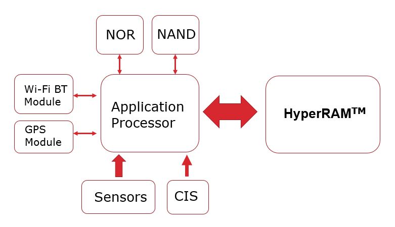
Fig.1 mobile device block diagram
| SDRAM | LPSDRAM | CRAM/pSRAM | HyperRAM™ | |
|---|---|---|---|---|
| Standard Published Time | 1994 | 2007 | 2005 | 2019(2.0), 2014(1.0) |
| Logic process node when standard published | 800nm | 65nm | 90nm | 7nm |
Table 1
HyperRAM™,which supports the HyperBus™ interface, is a latest technical solution to address this demand. HyperBus™ technology was first unveiled by Cypress in 2014, and the company launched its first HyperRAM™ product in 2015. By seeing the market demand, Winbond Electronics has decided to join the HyperRAM™ camp and launches 32Mb/64Mb/128Mb density products.
Benefits of using HyperRAM™
HyperRAM™ has only 13 signal IO pins, which can greatly simplify the PCB layout design. It also means that when designing end products, it allows MCU to have more pin out for other purposes or allows MCU with fewer pins for better cost-effectiveness. As Fig.2 shows, HyperRAM™ has fewest pins to achieve approximately the same throughput (333MB/s), compared to similar DRAM, like Low Power DRAM, SDRAM and CRAM/PSRAM.
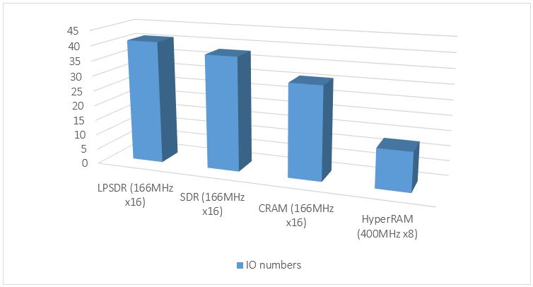
Fig.2 IO Pins Comparison
Simplifying control interface is another feature of HyperRAM™. PSRAM only has 9 states compared to 18 ones of LPSDRAM. The fewer the flow state, the less complexity the DRAM controller requires. The detailed difference could be referred as Fig.3. For instance, based on PSRAM architecture, HyperRAM™ is a self-refresh RAM. Moreover, it can automatically return to standby mode. Therefore, system memory is easier to be used, and the development of firmware and drivers is also simplified.
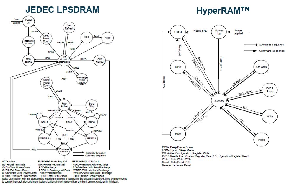
Fig.3 The difference of state flow between LPSDR and HyperRAM™
Owing to the fact that HyperRAM™ has been developed in recent years, it could utilize the newest semiconductor process node and package technology, which leads to its package size is smaller than any DRAM else . Fig.4 is the comparison between SDRAM size defined by JEDEC, PSRAM and HyperRAM™.
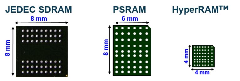
Fig.4 Comparison of package size
The key to IoT device
Power consumption is critical to IoT devices, since they are usually powered by the battery. Reducing power consumption not only save used energy but also reduce the cost of recharging and of replacement. Take Winbond's 64Mb HyperRAM™ as an example, the power consumption of Standby is 90uW@1.8V, while that of the same capacity SDRAM is about 2000uW@3.3V. More importantly, power consumption of HyperRAM™ is only 45uW@1.8V in Hybrid Sleep Mode, which is a significant difference from that in Standby mode of SDRAM (Table 2). On the other hand, even Low Power SDRAM is adopted, power consumption and form factor are both still bigger than that of HyperRAM™.
| SDRAM | CRAM | LPSDRAM | HyperRAMTM | HyperRAMTM (Hybrid Sleep Mode) | |
|---|---|---|---|---|---|
| Voltage(V) | 3.3 | 1.8 | 1.8 | 1.8 | 1.8 |
| Standby Power(uW) | 2000 | 400 | 160 | 90 | 40 |
Table 2 Power Consumption Comparison
New force of HyperRAM™ ecosystem
Since traditional SDRAM and PSRAM have matured, they are hardly to be optimized for emerging IoT applications. Considering the long-term supply requirements for automotive and industrial applications, the advanced process nodes of Winbond's HyperRAM™ can meet customers' longevity product lifecycle.
From the perspective of overall system design and product life, HyperRAM™ has become an ideal choice for emerging IoT devices. In addition to Cypress, leading MCU companies such as NXP, Renesas, ST, and TI have already provided MCUs that support HyperBusTM interface, and their new products will continue to support it in the future.
Meanwhile, its development platform of control interface is ready. Cadence and Synopsys have also begun to provide HyperRAM™ memory verification IP, which can accelerate IC vendors' design cycle. As a result, compared to other Octal RAMs, HyperRAM™ has the most mature application environment. HyperRAM™ has been incorporated into JEDEC standard, becoming a JEDEC xSPI compatible technology.
The current status of Winbond's HyperRAM™ product line is: 32Mb, 64Mb and 128Mb have entered mass production. Products of 24BGA (automotive grade), 49BGA, WLCSP and KGD are available. Size of 24BGA is 6x8 mm2, while that of 49BGA is only 4x4 mm2, which targets the consumer wearable market. Winbond has more than 20-year experience of manufacturing DRAM. Look to the future, Winbond will keep providing best products to meet customer needs.


 English